
GeSn(0.524 eV)single-junction thermophotovoltaic cells based on the device transport model
2022-05-16 07:12XinMiaoZhu朱鑫淼MinCui崔敏YuWang汪宇TianJingYu于添景JinXiangDeng邓金祥andHongLiGao高红丽
Chinese Physics B 2022年5期
Xin-Miao Zhu(朱鑫淼) Min Cui(崔敏) Yu Wang(汪宇) Tian-Jing Yu(于添景)Jin-Xiang Deng(邓金祥) and Hong-Li Gao(高红丽)
1Faculty of Science,Beijing University of Technology,Beijing 100124,China
2Department of Physics,Faculty of Science,Kunming University of Science and Technology,Kunming 650500,China
Keywords: GeSn,thermophotovoltaic device,active layer,photovoltaic cell
1. Introduction
Over the past few decades, thermophotovoltaics(TPVs)[1–6]have received increasing interest due to their excellent characteristics such as high energy conversion efficiency, superior output power, compactness, etc. The need exists with TPV cells to increase their efficiency with narrow band gap (0.5 eV–0.7 eV)[7]engineered materials compatible with economical substrates. Compared with conventional TPV materials, GeSn provides a tunable narrow band gap(0.5 eV–0.66 eV) by controlling the Sn content in directtransition semiconductors with increasing Sn concentration,higher carrier mobility and epitaxial fabrication for large-scale Si processes.[8]Therefore, these advantages of GeSn suggest the potential application of GeSn in TPV devices.
However,epitaxial growth of GeSn crystals is very challenging because of the huge lattice mismatch between Ge andα-Sn (14.7%), the surface segregation of Sn in Ge[9]and the extremely low equilibrium solubility of Sn in Ge(~1%).[10]Recently,many research groups have successfully fabricated high-quality GeSn epitaxial films[11–13]and GeSn photodetectors,[14,15]but photovoltaic research on GeSn is still in its initial stage. Conleyet al.[8,16]have manufactured highquality GeSn films on Si using a relaxed Ge buffer layer,which can be used in high-efficiency multi-junction PV and TPV cells. The relaxation of strain in GeSn alloys with a higher Sn content(12%)has been investigated by Kondratenkoet al.,[17]with promising results for GeSn PV cell applications. Up to now,there have been few investigations into GeSn TPVs. It is thus urgent to study GeSn for TPV applications both theoretically and experimentally.
In this paper, based on the transport equation for semiconductor devices, we focus on studying the dependence of thermal radiation conversion performance on the active layer and black-body temperature using a 0.524 eV GeSn TPV cell as an ideal diode. Four concrete configurations, p–on–n and n–on–p stacks in normal and inverted form,were investigated and compared. The results of this work can offer many profitable guidelines for the development of related TPV cells.
2. Model and simulation
A previous report[18]stated that direct band gap GeSn(0.524 eV)with a Sn content of 10%has been fabricated;we use this as our study material. Four GeSn single-junction TPV cells with p+/n,n+/p,p/n+,and n/p+structures,respectively,were studied. For each structure,an ideal diode was extracted from its practical condition as the device active layer. The effects of surface photonic reflection loss,front electrode shadowing and parasitic resistance on cell performance have been neglected in this work. On the basis of the classical photovoltaic cell model,[19]the current density(J)–voltage(V)characteristics are given as

whereλandλmare the incident wavelength and cutting wavelength,respectively.φ(λ)is the irradiation spectrum of incident light andQE(λ)is the internal quantum efficiency,which can be found in the classical text of Sze and Mattis.[19]φ(λ)is described in terms of Plank-like black-body irradiation as

whereμmin,e/h/μmax,e/hdenotes the value of electron/hole minority carrier mobility at the exceedingly low (high) doping density,αe/his the suggested fitting parameter andNref,e/hrepresents the doping concentration at which the mobility is decreased to half the value it reaches for low doping at room temperature.Le/hin Eq.(6)is given as

whereBopt,τSRH,e/h, andΛare the radiation recombination coefficient,trap-assisted recombination lifetime and Auger recombination coefficient,respectively.
Therefore, after obtaining theJ–Vcharacteristics of the photovoltaic device and combining it with the total powerσT4BB, whereσis the Stefan–Boltzmann constant,ηfor the TPV cell can be obtained. Table 1 shows the simulation parameters derived from experimental data used in this work.

Table 1. Some model parameters used in simulation.
3. Results and discussion
Generally, the specific structure of a diode active layer can be constructed in the p–on–n or n–on–p configuration.Depending on the highly doped layer in the front(emitter)or rear(base) layer of diode, a normal or inverted structure can be further obtained for each configuration. To reveal the electricity generation controlled by the active layer, taking the doping profile at 1019(1017) cm-3for the highly (lightly) doped layer, we have systematically researched the thickness evolution of the active layer on power conversion efficiency with aTBBof 1500 K.The calculated results for the p–on–n configuration are shown in Fig.1. It can be observed in Fig.1(a)that with increasing thickness of the emitter,ηdemonstrates only a slight improvement initially and then a rapid decline. As the base thickness increases,ηincreases rapidly then slowly.As described in Fig. 1(b), when the base thickness is 15 μm,the emitter increases to 0.09 μm, which gives the maximum conversion efficiency. Meanwhile,figure 1(c)shows that with increasing thickness of the base,ηis enhanced from steeply increasing to flat and then increases to saturation; when the base is 5.4 μm thick a suboptimumηof 5.17% is obtained.We found that the cell showed higher efficiency with a thinner emitter and a thicker base, because the emitter plays a major role in the conversion efficiency. The emitter region can easily absorb high-energy photons and has a very small penetration depth, while the base region can more easily absorb long-wavelength photons and has a larger penetration depth.Moreover,the smaller thickness of the optimal emitter can be ascribed to a shorter minority carrier diffusion length due to the higher doping concentration in the emitter region. More significantly,in contrast to the optimum structure,the employment of quite a few suboptimal configurations is not remarkably degrading. From the viewpoint of designing an economical structure using fewer materials,a suboptimal structure can be a better choice.
In comparison with p+/n,the results for the p/n+configuration are different, as shown in Fig. 1(d). As the emitter thickness increases,ηimproves initially and then decreases,and with increasing base thickness,ηdisplays an initial rapid enhancement and then tends to be stable. Specifically, as can be seen in Fig.1(e),the critical emitter thickness is 0.54 μm.Figure 1(f)shows that the base thickness with a tendency to increase to saturation is approximately 3.6 μm,and this presents a suboptimumηof 4.24%. In contrast to the optimal normal configuration, the entire cell thickness is reduced. Thus, the degradation of the absorption spectrum results in a decrease ofη. For the inverted case, there is an increase in the optimum emitter thickness compared with the normal configuration. Physically,when reducing the doping profile of a device emitter, enlargement of the minority diffusion lengthLerequires a thicker emitter.

Fig. 1. Efficiency versus active layer thickness for p+/n (a) and p/n+ (d) configurations. For p+/n and p/n+ structures, the base thickness respectively is 15 μm(b)and 10 μm(e),η versus the emitter thickness;the emitter thickness respectively is 0.09 μm(c)and 0.54 μm(f),η versus the base thickness.
The n–on–p configuration as a function of active thickness is schematically described in Fig.2. The dependence ofηon the active layer thickness for the n+/p device is shown in Fig. 2(a). With increasing emitter thickness, a peak value ofηis observed,and as the base thickness increases,ηdisplays an initial rapid increase and then tends to saturation,which is consistent with the normal p+/n structure. It can be observed in Fig. 2(b) that when the base thickness is 12 μm, a critical emitter thickness of 0.024 μm is observed, which gives the maximum value ofη. Figure 2(c) shows that when the base thickness increases to about 3.48 μm, a suboptimalηof 4.59% is achieved. The results can be understood as follows: sinceμein the p-type emitter is smaller thanμhin the n-type base,promoting the collection of minority electrons in the front layer,the resulting smallLerequires a thinner emitter.To compensate for the absorption loss caused by the thinner emitter, the base thickness should be appropriately enlarged for better spectral utilization. Compared with the n+/p configuration, the results for the n/p+structure are diverse. As depicted in Fig.2(d),with increasing emitter thickness,an initial increase and then a reduction inηwas observed. To be specific,ηis plotted as a function of the emitter thickness in Fig. 2(e), where the optimum emitter thickness is 0.39 μm,and as shown in Fig.2(f)the base thickness tends to increase to saturation at approximately 2.48 μm,giving a suboptimalηof 4.04%.
In contrast to Figs.1 and 2,we can see that the output performance of the inverted configuration is inferior to the normal one,and the p+/n structure shows an optimal conversion efficiency.Physically,for the p+/n construction,a higher minority carrier(electrons)mobility in the highly doped emitter makes it easier to collect photogenerated charge carriers. In the normal p+/n construction, a reasonable active layer can be composed of a 100 nm–300 nm emitter and a 3 μm–6 μm base.These results for the configuration and active layer thickness can give useful guidelines for the GeSn TPV cell experiment.

Fig.2. Active layer thickness-dependent efficiency for n+/p(a)and n/p+ (d)structures. For n+/p and n/p+ configurations,the base thickness is 12 μm(b)and 8 μm(e),respectively,the emitter thickness-dependent η;the emitter thickness is 0.024 μm(c)and 0.39 μm(f),respectively,the base thickness-dependent η.
To further reveal the doping versus cell output characteristic, we can tuneNd(a)in the lightly doped layer of the optimal configuration. The evolution ofJ0andJscwith doping level is schematically displayed in Fig. 3. As shown in Fig. 3(a), with increasing doping,J0presents an initial dramatic reduction and then tends to saturation. The degradation ofJ0can be attributed to the inverse relationship between the doping concentration andJ0(as shown in Eq.(6)). As can be seen from Fig.3(b),Jscfor the p+/n(n+/p)configuration decreases from 14.53(14.47)A·cm-2forNd(a)=1×1017cm-3to 13.72 (14.09) A·cm-2forNd(a)=9×1018cm-3. In the same doping range,Jscfor the inverted structure decreases from 13.83 (14.01) A·cm-2withNd(a)of 1×1017cm-3to 13.07(12.81)A·cm-2withNd(a)of 9×1018cm-3for the p/n+(n/p+)configuration. The weak degradation for each structure can be ascribed to the reduction ofτe/hdue to the increased doping. Thus,a reasonable doping level would improve TPV electricity generation.
Meanwhile, the corresponding characteristics ofVoc, fill factor (FF), andηas a function of the doping profile in the lightly doped layer for the optimum construction are evaluated in Fig. 4. Figure 4(a) shows thatVocimproves initially and then tends to be stable with increased doping. Specifically,Vocfor the p+/n structure can be increased from 0.19 V forNd=1×1017cm-3to 0.27 V forNd=6×1018cm-3and then slightly diminishes,whileVoc(≈0.26 V)for the n+/p configuration manifests extreme enhancement in the initial stage and then saturates at a higher doping level. As shown in Fig.4(b),with variation in doping level, FF is highly consistent with the observedVoc. Consequently,ηshows a distinct augmentation accompanying the upgraded doping in Fig. 4(c). For the p+/n(n+/p)construction,ηdisplays an initial observable improvement when doping in the base region increases from 1×1017cm-3to 3(7)×1018cm-3,for which a maximumηcan be observed. A further increase in doping induces a slight reduction inη.These results are similar to the literature results for the 0.53 eV GaInAsSb TPV diode described by Wang and Lou.[31]For the p/n+(n/p+)construction,ηslowly improves from 4.28% (4.34%) withNd(a)= 1×1017cm-3to 8.62%(8.49%)withNd(a)=9×1018cm-3. Under the same doping profile,the conversion efficiency of the normal construction is higher than that of the inverted one, which can be attributed to sufficient utilization of the spectrum due to the improved active layer thickness in the normal structure. Hence,with increasing doping, the enhancement ofηis dominated by the increasingVoc.

Fig.3.The J0(a)and Jsc(b)of the optimum configurations versus the doping concentration in the lightly doped layer.

Fig.4. The Voc (a),FF(b),and η (c)of the optimum configurations versus the doping concentration in the lightly doped layer.
Since the radiation characteristic of an intermediate radiator can be controlled by artificial engineering, it is worth evaluating the potential effect of radiator temperature on device output performance of the optimal configuration. Figure 5 shows the photon flux(a)as a function of wavelength at differentTBB, andJsc(b),Voc(c), FF (d), POD (e), andη(f)versus the variation ofTBBfor our considered configurations have been studied.As can be seen from Fig.5(a),with increasingTBB,the photon flux displays remarkable enhancement and a blue shift of the radiation peak was observed. In addition,GeSn (0.524 eV) with a cutoff wavelength of 2.36 μm was observed in the near-infrared band where it can capture most thermal radiation of photons from a black-body at 1500 K;this would facilitate the use of GeSn material in TPV cell applications. Figure 5(b) shows thatJscshows exponential enhancement with the increasingTBB. To be specific,Jscimproves from 1 A·cm-2forTBB=1000 K up to 170 A·cm-2forTBB=2500 K,which can be attributed to the enhancement of photon flux owing to the increasedTBB. BothVocand FF for each structure display evident improvement with the upgradedTBB. For the p+/n construction,Voc(FF)in Figs. 5(c)and 5(d) increases from 0.12 V (53.87%) forTBB=1000 K up to 0.26 V (69.13%) forTBB=2500 K. The enlargement ofVoccan be understood because the increasingTBBresults in improved carrier collection,which can improve the band state,further leading to the band-filling effect[31,32]and slight augmentation ofVoc. For the normal structureVocis invariably larger than for the inverted one,which can be attributed to the smallerJ0for the normal one. The improvement of FF can be attributed to the increasedTBB,and is derived from the empirical formula[33]FF = [Voc-ln(Voc+0.72)]/(1+Voc). Figure 5(e) shows that POD displays exponential improvement with increasingTBBdue to the combined effect ofJsc,Voc,and FF (POD=Jsc×Voc×FF). Moreover,ηof the p+/n (n+/p)configuration increases from 1.22%(1.07%)forTBB=1000 K to 14.05%(13.28%)forTBB=2500 K;in the sameTBBrange,ηfor the n/p+(p/n+) configuration increases from 0.65%(0.69%)to 10.46%(10.89%), as shown in Fig.5(f). Accordingly,an almost linear increase inηwas observed,presenting a 12–16-fold improvement and revealing the significance of controllableTBBfor TPV devices.
We know that surface recombination is a very important parameter for TPV cells. To reveal the potential effect of surface recombination rates, using the p+/n configuration as an example,we have depicted TPV performance parameters versus the variablesSBandSFin Fig. 6, whereSBandSFof the optimal structure are equivalent to aTBBof 1500 K. In Fig. 6(a), it is obvious that the concernedηvaries when the value ofSF/Bis in the range of 103cm·s-1–107cm·s-1. The analogous behavior for other parameters such asJsc,Voc, FF,and POD is also shown in Fig.6. Cell performance would be improved with decreasingSF/B,In particular,cell performance decreases at high(107cm·s-1–1010cm·s-1)surface recombination rates,but low(101cm·s-1–103cm·s-1)surface recombination rates give a higher thermoelectric conversion performance,indicating the significance of good quality contacts in practical TPV applications. A feasible way to reduceSF/Bis by passivating the surface of the device to remove the recombination resource formed by surface impurities;this is helpful for improving cell conversion efficiency.[34]
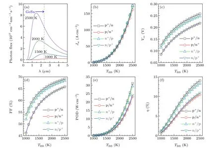
Fig.5. Photon flux per unit wavelength at different TBB (a),and dependence of the optimal structure Jsc (b),Voc (c),FF(d),POD(e),and η (f)on various values of black-body illumination.

Fig.6. Device performances of Jsc,Voc,η (a)and FF,POD(b)with variation of SF/B.
4. Conclusion
In this paper, we have systematically studied the effects of the active layer on the output performance of GeSn singlejunction TPV cells with normal and inverted configurations.The results show that GeSn TPV cells with acceptable performance consisting of a 100 nm–300 nm emitter and a 3 μm–6 μm base with low device cost and the optimal p+/n structure have been obtained. In the p+/n (n+/p) structure, there is an optimum base dopingNd(a)=3(7)×1018cm-3.Performance of the GeSn TPV cells can be improved by increasing the radiator temperature and decreasing surface recombination. The simulated results provide some useful guidelines for the fabrication of economical GeSn TPV devices.
Acknowledgment
Project supported by the Beijing Natural Science Foundation Program,China(Grant No.4192016).

- Chinese Physics B的其它文章
- A nonlocal Boussinesq equation: Multiple-soliton solutions and symmetry analysis
- Correlation and trust mechanism-based rumor propagation model in complex social networks
- Gauss quadrature based finite temperature Lanczos method
- Experimental realization of quantum controlled teleportation of arbitrary two-qubit state via a five-qubit entangled state
- Self-error-rejecting multipartite entanglement purification for electron systems assisted by quantum-dot spins in optical microcavities
- Pseudospin symmetric solutions of the Dirac equation with the modified Rosen–Morse potential using Nikiforov–Uvarov method and supersymmetric quantum mechanics approach