Study on the photo response of a CMOS sensorintegrated with PIN photodiodes
2019-10-22 11:29YANGChengcaiJUGuohaoCHENYongping
中国光学 2019年5期
YANG Cheng-cai,JU Guo-hao,3,CHEN Yong-ping
(1.Key Laboratory of Infrared Imaging Materials and Detectors,Shanghai Institute ofTechnical Physics,Chinese Academy of Sciences,Shanghai 200083,China; 2.University of Chinese Academy of Sciences,Beijing 100049,China; 3.School of Information Science & Technology,Shanghai Tech University,Shanghai 201210,China)
*Corresponding Author, E-mail:chen_yp@mail.sitp.ac.cn
Abstract: Traditional CMOS image sensors generally use PN photodiodes or PPDs as the photosensitive element, which are formed based on N-well/P-type substrates using the LV-CMOS process. The PIN photosensitive element has small junction capacitance and high quantum efficiency. By using High-Voltage CMOS(HV-CMOS), monolithic integration of CMOS circuits with PIN photodiodes can be achieved. In this paper, the relationship between the photo-response characteristics, NEP of CMOS detectors and pixel size and reset voltage are studied. The results show that the pixel charge gain can be increased by about one order of magnitude when the photosensitive element is changed from PN to PIN and the transient charge gain of the pixel is larger than 1/Cpd. This is closely related to the size of the diode and reset voltage. It is found that small pixels are more suitable for fast detection of short integration time under weak signals because of their higher charge gain and lower equivalent noise. If combined with microlenses, small pixels can be further advantageous in low light detection.
Key words: CMOS image sensor;HV-CMOS;PIN photodiodes;3T pixel structure
1 Introduction
Low light level imaging is an optical imaging process under conditions with low illumination(below 10-2lx). It plays an important role in aerospace, meteorological observation and military reconnaissance[1-4]. With the development of CMOS technology, CMOS image sensors began to replace CCDs and gradually extended to the field of low-light-level imaging[5-7]. At present, the most commonly used CMOS image sensor generally uses 3T or 4T pixel structures with photodiodes based on PN type due to the limitation of CMOS process compatibility. 4T pixels can achieve higher sensitivity and lower noise due to the addition of a charge transfer transistor and readout floating capacitors, but it also limits the size of pixels and are not suitable for the development of large pixel devices. The PIN photodiode is a special form of PN photodiode. It has the advantages of small junction capacitance, fast response speed, high quantum efficiency and no absolute restriction on pixel size[8]. However, the fabrication of PIN photosensitive elements is not compatible with the standard low voltage CMOS process(LV-CMOS). At present, most of the research on the integration of PIN photosensitive elements and CMOS circuits is based on SOI process[9-10].
In this paper, the photo-response characteristics of CMOS image sensors with a PIN photodiode as the photosensitive element in HV-CMOS processes are analyzed, with special attention given to the effects of pixel size and reset voltage on the photo-response characteristics and the noise equivalent power(NEP) of the detector.
2 HV-CMOS process
Compared with the standard LV-CMOS process, the HV-CMOS process(shown in Fig.1) adds a lightly doped p-type epitaxial layer with a thickness of about 20 μm and a resistivity of 400~1 000 Ω·cm to the heavily doped p-type substrate. At the same time, in order to meet the low resistivity requirement(1~10 Ω·cm) of the substrate of CMOS circuits, deep N-wells were fabricated on the p-type epitaxial layer in the MOS region before the fabrication of the PMOS and NMOS. Then the CMOS circuit was fabricated on the deep N-wells using the standard LV-CMOS process, while photosensitive elements were fabricated directly on the high-resistivity p-type epitaxial layer. In this way, monolithic integration of a PIN photosensitive element and a CMOS circuit was formed(shown in Fig.2)[11].
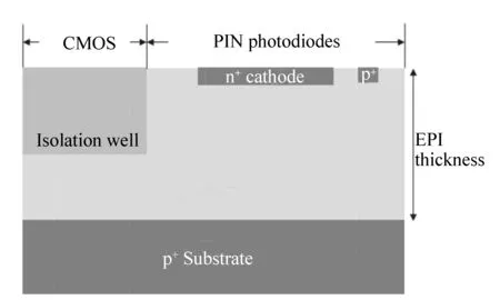
Fig.1 Schematic diagram of HV-CMOS process 图1 HV-CMOS工艺示意图
CMOS circuits fabricated through this process can operate at high voltages. Now,this process is one of the standard CMOS fabrication processes.
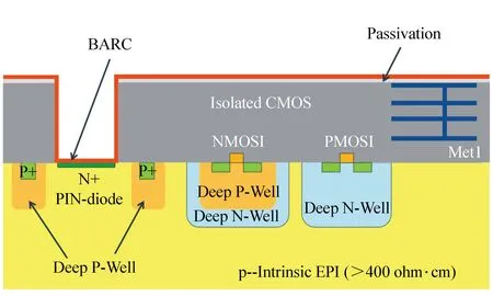
Fig.2 Monolithic integration of PIN photosensitive element and CMOS circuit 图2 PIN光敏元与CMOS电路单片集成
In this process, PIN photodiodes consist of a heavily doped p(p+) region (P layer), a lightly doped p(p-) epitaxial layer(I layer) and a heavily doped n(n+) region(N layer). The existence of the intrinsic layer(I layer) increases the width of the depletion region and quantum efficiency of the diode, which is the fundamental reason that the sensitivity of PIN photodiode is higher than that of the PN photodiode. On the other hand, the thick dielectric layer formed on the surface of PIN photosensitive element can be removed in this process and the quantum efficiency of the photosensitive element can be further improved by replacing it with a single layer of antireflection coating.
3 3T pixel structure
The CMOS sensor with a PIN junction as the photosensitive element can use a 3T pixel structure(shown in Fig.3). This structure is advantageous for its simple structure and high filling factor[12]. In the pixel structure, the PIN photodiode is the only photosensitive part of the whole CMOS image sensor; M1 is a reset transistor, through which the photodiode is reset to the reverse bias voltage value when the signal is read out; and M2 is a follower transistor, responsible for the pixel signal readout. In order to reduce the effect of charge injection, the size of the reset transistor should be as small as possible.
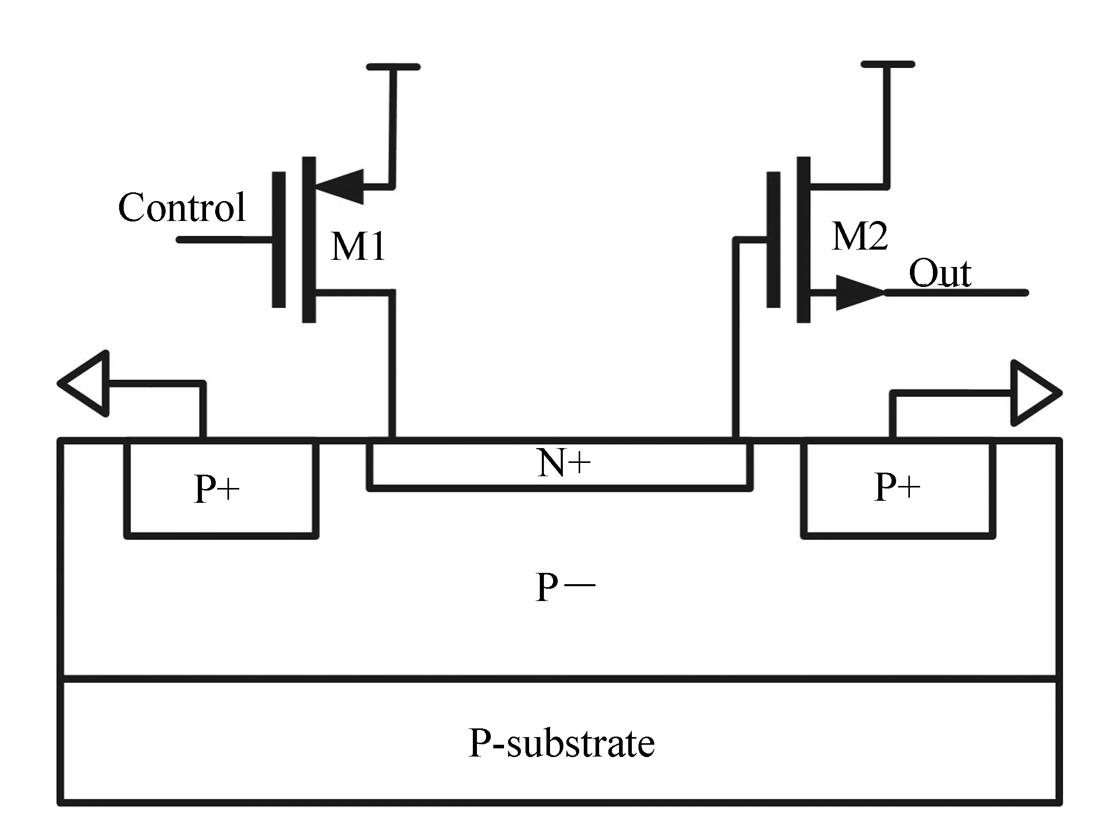
Fig.3 3T pixel structure in HV-CMOS process 图3 HV-CMOS工艺中的3T像素结构
Compared with the 3T pixel structure, the 4T pixel adds a charge transfer tube and a floating capacitor which needs a special design behind the photodiode for it to achieve true correlation double sampling. However, this also makes the 4T pixel production process complex and costly. Furthermore, in order to achieve higher sensitivity, the capacitance of the floating capacitor is smaller, which makes it inconducive to the development of large-pixel devices.
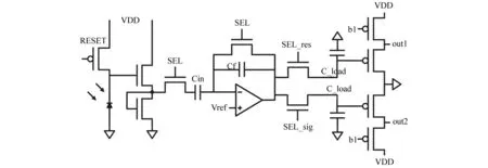
Fig.4 Read-out circuit in CMOS sensor 图4 CMOS传感器读出电路
Pixel signal readout requires a column level circuit for further amplification and sampling output(shown in Fig.4). The circuit mainly includes a CTIA(Capacitive Transimpedance Amplifier), an amplifier(for signal amplification), sample and hold circuits(for correlation double sampling) and source followers(for output drive).
4 Detector performance analysis
4.1 Differences in structure and process
The standard LV-CMOS process provides a PN photodiode structure based on a low resistivity P-substrate and an N-well. Both PMOS and NMOS are fabricated in wells(Twin-well process). Compared with the PIN photodiodes in the HV-CMOS process,the space charge region(depletion layer) of the two photosensitive elements is quite different(shown in Fig.5), which introduces significant changes to the photo response characteristics of PIN and PN photodiodes.
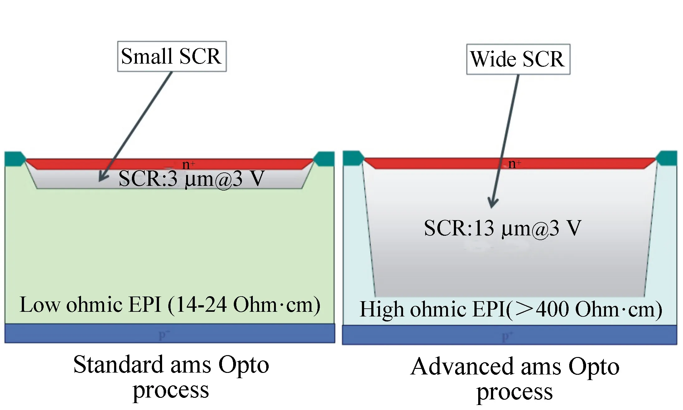
Fig.5 Space charge regions of PN and PIN 图5 PN和PIN空间电荷区
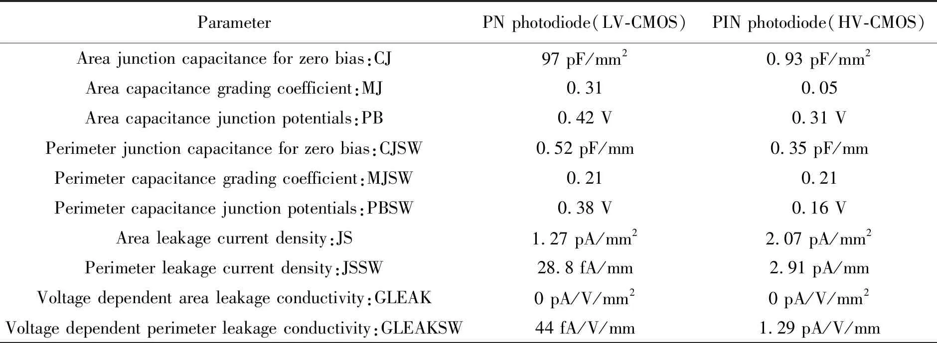
Tab.1 Formula parameters
4.2 Junction capacitance and dark current
Junction capacitance and dark current are two important characteristics of photodiodes, in which junction capacitance is related to charge conversion gain, while dark current mainly affects the dynamic range of the detector and introduces shot noise.
The junction capacitance and dark current of PN and PIN photodiodes in the standard LV-CMOS and HV-CMOS processes can be expressed in formulas (1) and (2), respectively.

(1)
Id=(JS+GLEAK·V)·WL+
(JSSW+GLEAKSW·V)·2·(W+L) ,
(2)
whereWandLare the dimensions of a diode′s cross section andVis the reverse bias voltage of the photodiode. At room temperature, the parameters of different processes are shown in Tab.1.
To simplify the analysis, the photodiode′s cross section is set to a square such thatW=L. Using formula 1, the relationship between junction capacitance and bias voltage(V) of different pixel sizes(L)(shown in Fig.6) and between junction capacitance and pixel size(L) of different bias voltages(V)(shown in Fig.7) can be obtained.
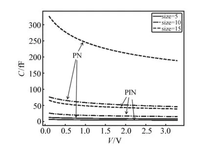
Fig.6 Relationship between junction capacitance and bias voltage 图6 结电容随偏压变化关系
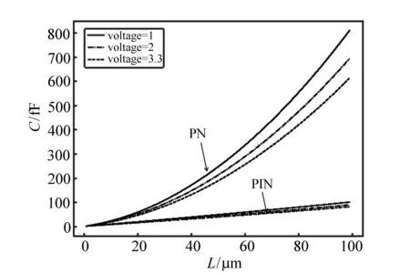
Fig.7 Relationship between junction capacitance and pixel size 图7 结电容与像素大小的关系
It can be seen that the junction capacitance of the PN photodiode is larger than that of the PIN photodiode with the same area and bias voltage. In large pixels(L>80 μm), the junction capacitance of the PN photodiode is almost one order of magnitude larger than that of the PIN photodiode. Even in small pixels(L≈20 μm), the junction capacitance of the PN photodiode is also about 5 times of that of PIN photodiode. The junction capacitance of both of them varies obviously at low voltages(<1 V) while it varies little when the voltage is higher than 2 V. As shown in Fig.7, the junction capacitance of the PIN photodiode is linear with the length of the pixel, while the junction capacitance of PN photodiode is quadratic. This shows that the junction capacitance is mainly determined by the perimeter capacitance in the PIN photodiode, while the junction capacitance of the PN photodiode is mainly determined by the area capacitance. At the same time, the junction capacitance of the PIN is mainly determined by the perimeter capacitance, which indicates that the photosensitive element with small pixels also has a wide depletion region in the transverse direction. As a result, smaller photodiodes can achieve the same quantum efficiency as larger photosensitive surfaces.
Using formula 2, the relationship between dark current and bias voltage at different pixel sizes(L)(shown in Fig.8), and the relationship between dark current and pixel sizeLat different bias voltages(shown in Fig.9) can be obtained.
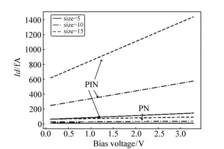
Fig.8 Relationship between dark current and bias voltage 图8 暗电流与偏置电压大小的关系
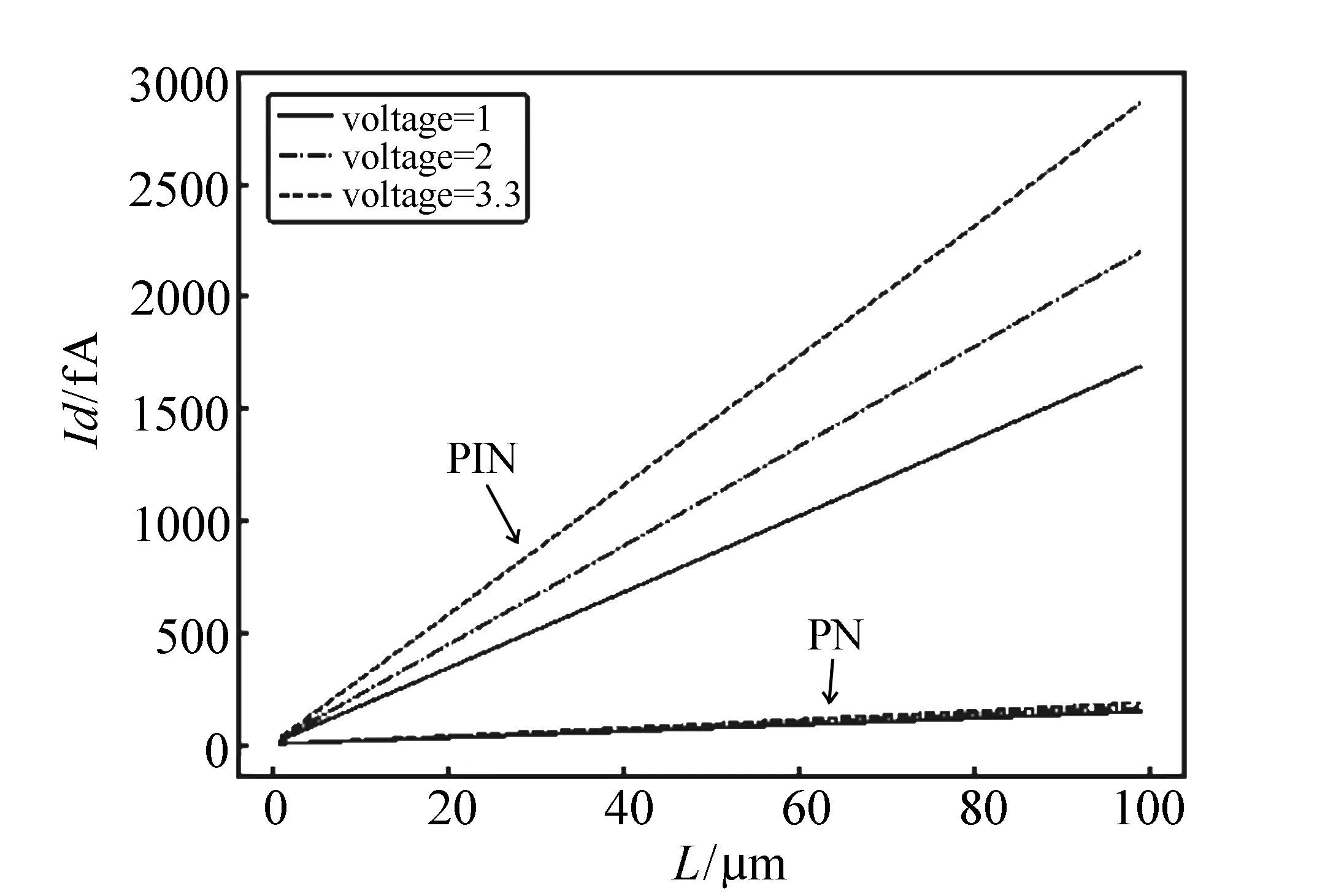
Fig.9 Relationship between dark current and pixel size 图9 暗电流与尺寸L的变化关系
It can be seen that under the same area and bias voltage, the dark current of a PIN photodiode is larger than that of a PN photodiode, generally 1-2 orders of magnitude higher. Therefore, in applications, PIN photodiodes need to be cooled. As shown in Fig.9, the dark current is linearly related to the lengthL, which indicates that the dark current is mainly composed of the perimeter leakage current.
4.3 Sensitivity of devices
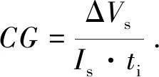
Charge conversion gainCGis one of the most important characterization parameters of a detector′s sensitivity, which reflects the effect of signal charge on junction voltage. Usually, the junction capacitance of a diode is considered as a planar capacitor. As a result, for a given signal charge ΔQ, the voltage variation ΔVon the junction capacitanceCpdsatisfies the following relationship:
ΔQ=Cpd·ΔV.
(3)
Therefore, the charge conversion gainCGequals to 1/Cpd[13].
For PIN photodiodes, the situation is more complicated. As analyzed earlier, the junction capacitance of a PIN photodiode varies with the bias voltage, especially at low bias voltages. This means that its junction capacitance is continuously changing during the integral process of the signal charge. It cannot be calculated using the method in formula (3). Instead, the numerical calculation method can be used.
The voltage variation ΔVcaused by the charge is the difference between the reset voltageVresetand the pixel voltageVpixel. When the parasitic capacitance of the reset transistor and the follower transistor is ignored, the photodiode satisfies the charge formula at any time:
Q=Vpd·Cpd.
(4)
The charge variation on the junction capacitor is the sum of the signal charge(Qs) and the dark current charge(Qd) from the start of reset to the integration timeti. That is,
Qs+Qd=(Is+Id)·ti,
(5)
therefore,
Vreset·CPd0-VPd·CPd=(Is+Id)·ti,
(6)
whereCpd0is the junction capacitance of the PIN photodiode at the initial time,Isis the photo current, andIdis the dark current. Accordingly,
Vpd·Cpd=Vreset·CPd0-(Is+Id)·ti.
(7)
Therefore, given the pixel size, fixed reset voltageVresetand integration timeti, the relationship curve between the junction voltageVpdand the photo currentIscan be obtained by numerical calculation(shown in Fig.10).
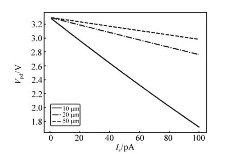
Fig.10 Relationship between junction voltage and photo current 图10 结电压与光电流关系
Fig.10 shows the variation of junction voltage with photo-current for different PIN photodiode sizes when the reset voltage is 3.3 V and the integration time is 100 μs. It must be noted that the variation of junction voltage includes the influence of dark current, and the influence of dark current need to be removed in order to obtain the variation of voltage caused by signal charge.
The voltage variation caused by the dark current is equal to the voltage variation when light is absent. That is:
ΔVd=Vreset-Vpd(Is=0) .
(8)
Therefore, the voltage change caused by the photo signal is:
ΔVs=Vreset-Vpd-ΔVd.
(9)
Using the above formula, under the same conditions as in Fig.10, the relationship between voltage variation and photocurrent(shown in Fig.11) can be obtained, which essentially varies linearly.
Therefore the average charge gainCGin an integral timetican be expressed as:
(10)
This reflects the average sensitivity of the integral charges, which is closely related to junction capacitance. Usually, small signal sensitivity needs to be considered. Specifically, that is the instantaneous charge gain of pixelsCG′:
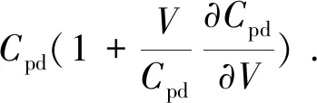
(11)
Since the junction capacitance of the PIN photodiode decreases with an increase of voltage(i.e., ∂Cpd/∂Vis a negative value) the transient charge gain of the pixel is higher than the reciprocal of the transient capacitance 1/Cpd, which is usually considered as charge gain.
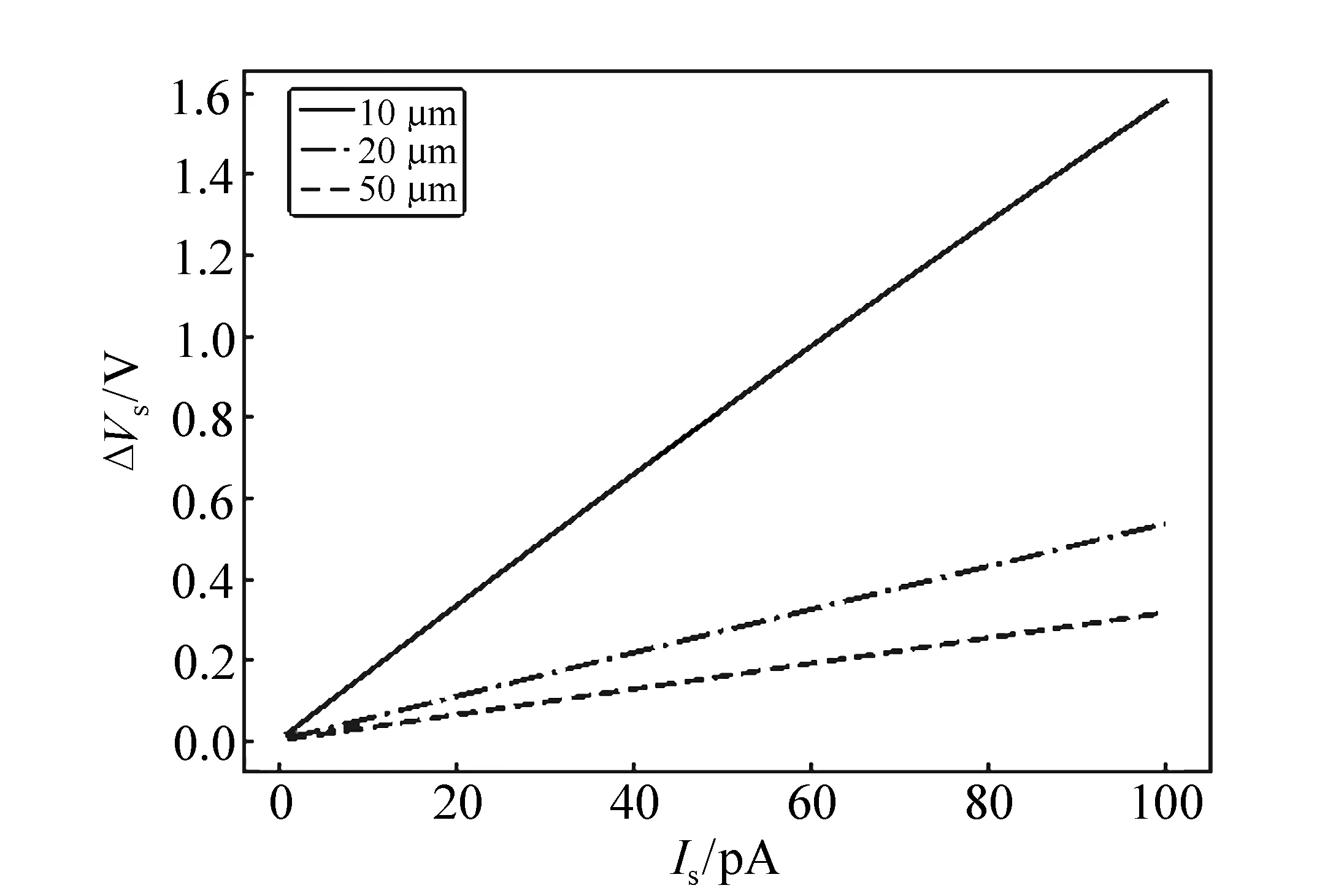
Fig.11 Relationship between photo signal voltage variation and photo current 图11 光信号电压变化与光电流关系
In Fig.11, although the independent variable is photo currentIs, since the integration timetiis fixed, the independent variable can be considered as signal charge. By deriving the curve, the transient charge gain curve in the process of self-integration(shown in Fig.12) is obtainable.
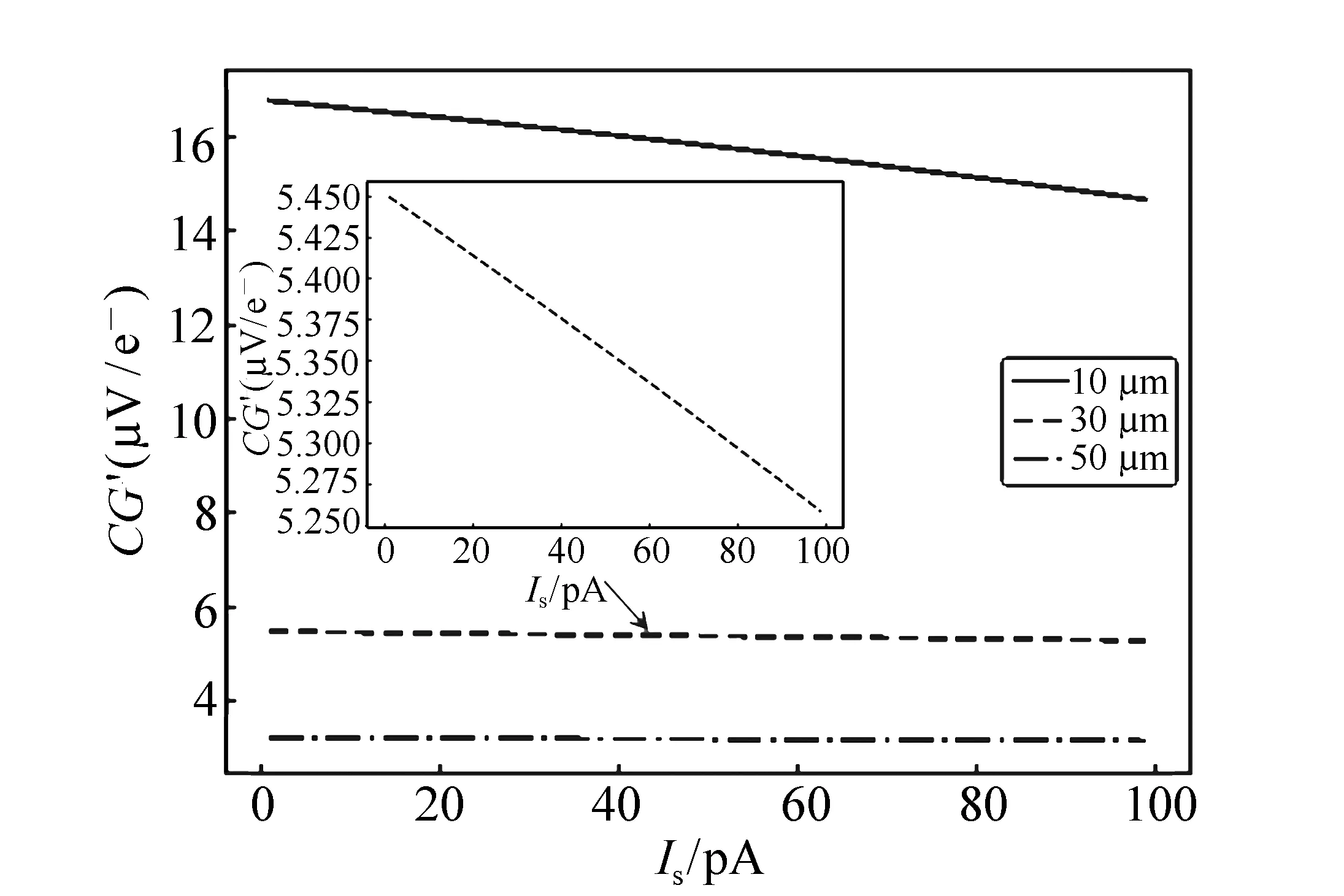
Fig.12 Relationship between transient charge conversion gain and photo current variance 图12 瞬态电荷转换增益随光电流变化关系
It can be seen from the graph that small pixels have a higher charge gain and that a small signal gain gradually decreases with the increase in photocurrent. This is more obvious with the small pixel. Therefore, in order to obtain higher pixel charge gain in low-light detection, smaller pixels should be selected.
Finally, we calculate the instantaneous junction capacitance of the pixel in the integration process and compare its reciprocal(1/Cpd) with the real instantaneous charge gain(shown in Fig.13). Here, the pixel size is 10 μm×10 μm.
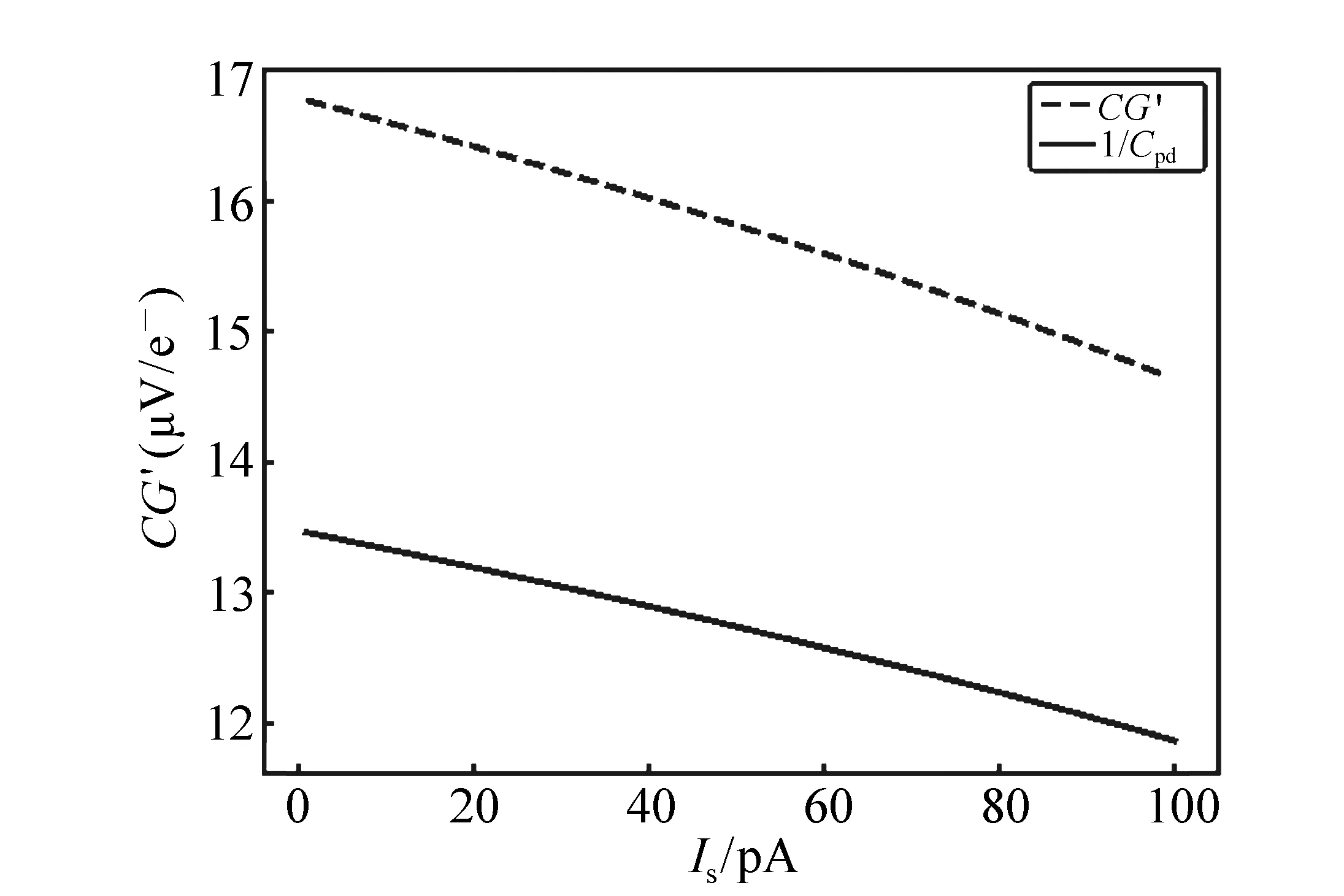
Fig.13 Comparison between transient charge gain and the reciprocal of capacitance value 图13 瞬态电荷增益与电容值倒数的比较
It can be seen that the transient charge gain of pixels is always greater than the reciprocal of junction capacitance, which is consistent with the analysis of Eq.11. Under 10 μm×10 μm pixel size, the instantaneous charge gain reaches 16 μV/e-. By using PIN photodiodes, we can not only obtain higher average charge gain(their capacitance is smaller than that of PN photodiodes) but also obtain higher transient charge gain than conventional methods. The transient charge gain of the pixel is the same as quantum efficiency, which reflects the charge sensitivity of the photosensitive element.
4.4 Noise analysis of devices
The equivalent input noise of the CMOS image sensor can be expressed as the sum of noise produced by pixel and noise produced by readout circuit:
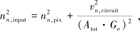
(12)
wherenn,pixis the number of noise electrons produced by PIN photodiodes,vn,circuitis the equivalent output noise voltage of the on-chip readout circuit,Atotis the total voltage gain of the on-chip circuit, andGeis the charge conversion gain of the PIN photodiode. HereGe=q·CG, whereqis the charge of electrons.
4.4.1 Noise of the PIN photodiode
The noise of the PIN photodiode mainly includes shot noise and reset(kTC) noise. Since the reset noise can be suppressed by correlated double sampling, the dominant one is shot noise. Shot noise is caused by the discreteness of the carriers that form the current, and is usually regarded as white noise. In PIN, shot noise is related to dark current and incident photon. The electron number of shot noise can be expressed as[14]:

(13)
In a certain integration timeti, the dark current noise electronsNdarkand photo-generated noise electronsNsigcan be expressed as
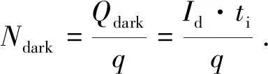
(14)
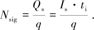
(15)
The photocurrent of a PIN photodiode can be expressed as the product of the current responsivityRi) and the incident light power(P),i.e.,
Is=Ri·P,
(16)
and the incident light power(P) can be expressed as the product of the light power per unit area(Ev) and the area of the photosensitive surface(l2,lis the length of the photosensitive surface):
P=l2·Ev.
Therefore, photocurrent can also be expressed as:
Is=Ri·l2·Ev.
(17)
4.4.2 The noise of the readout circuit
The readout circuit of a CMOS image sensor mainly includes a source follower, a CTIA amplifier and a sample and hold circuit.
The source follower is used to drive the output of the signal. It is used in two parts of the circuit, which are used for pixel signal readout and final output drive. The CTIA is the core part of the CMOS image sensor readout circuit, which mainly includes a single-ended cascode amplifier and a feedback loop composed of two capacitors, as shown in Fig.14.

Fig.14 Schematic diagram of a CTIA structure 图14 CTIA结构示意图
The total gainAtotof the CMOS image sensor readout circuit is the product of the gain of the above three parts, which is a fixed value before saturation. At the same time, the equivalent output noise voltage of the on-chip readout circuit can also be regarded as a constant at a given bandwidth[15]. In this paper, readout circuits are designed by the 0.35 μm HV-CMOS process.
4.5 Analysis of low light level detection capability of devices
Noise equivalent power(NEP) is the incident light power(P1) when the signal and noise are equal(SNR=1) in the detector,NEP=P1. According to the definition, the smaller the value, the better the detector performance.
When the signal-to-noise ratio(SNR) equals 1,Nsig=nn,input, wherenn,inputis the total equivalent input noise. Bringing the relevant formula to it,
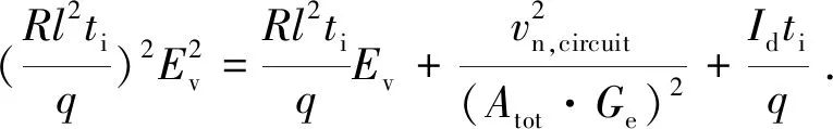
(18)
For convenience of calculation, the above formula can be rewritten as:

(19)
then, the solution can be obtained:
(20)
therefore,
NEP=P1=l2Ev.
(21)
Combined witha0=(Ril2ti)/q, it can be concluded thatl2/a0is a quantity independent of pixel size. Meanwhile, from the above analysis, we know that aslincreases,Gedecreases andIdincreases.a1also increases withl. So, the relationship between theNEPand the pixel size for integration times less than 100 μs, a 3.3 V reset voltage and 0.5 A/W current responsivity(shown in Fig.15) can be obtained. The results show that, for the detector integrated with a PIN photosensitive element and a CMOS circuit developed by the HV-CMOS process, when the pixel is 20 μm×20 μm, the device′s NEP can reach 0.08 pW in a short integration time(100 μs). This result is nearly 2 times lower than that of the detector of the same size developed by the standard LV-CMOS process.

Fig.15 Relationship between NEP and pixel size 图15 NEP与像素大小的关系
5 Conclusions
In this paper, a CMOS image sensor with 3T pixel structure integrated with PIN photosensitive elements was analyzed theoretically and the relationship between photo-response characteristics and noise equivalent power and the pixel size and bias voltage were studied in depth. The results show that generally, the junction capacitance of a PIN diode is about one order of magnitude lower than that of a PN diode, meaning that the PIN photodiode has higher charge conversion gain. Meanwhile, its transient charge gain is higher than 1/Cpd. Therefore, the equivalent input noise of a detector integrated with PIN photosensitive elements should be one order of magnitude lower under the same readout circuit. Because smaller pixels have smaller junction capacitance and dark current, they also have smaller NEP. This research should be instructive for the design of low-light level detectors.
——中文对照版——
1 引 言
微光成像是指在低照度(照度<10-2lx)环境中的光学成像过程。在航空航天、气象观测以及军事侦查等领域,微光成像技术都发挥着极为重要的作用[1-4]。随着CMOS工艺的发展,CMOS图像传感器开始替代CCD,逐步向微光成像领域扩展[5-7]。目前,由于CMOS工艺兼容性的限制,最为常用的CMOS图像传感器一般采用3T或4T像素结构,并且光电二极管均是以PN型为基本构成。4T像素由于增加了电荷转移管和读出浮置电容,可以实现更高的灵敏度和更低的噪声,但同时也限制了像素的大小,不适合大像素器件的研制。PIN光电二极管是PN结光电二极管的特殊形式,具有结电容小、响应速度快、量子效率高等优点[8],对像素大小也没有绝对的限制。但PIN光敏元的制作与标准低压CMOS工艺(LV-CMOS)不兼容。目前,对PIN光敏元与CMOS电路集成的研究大多基于SOI工艺[9-10]。
在本文中,将对采用HV-CMOS工艺的以PIN光电二极管为光敏元的CMOS图像传感器的光电响应特性进行分析,重点研究像素尺寸与复位电压对探测器光电响应特性和噪声等效功率(NEP)的影响。
2 HV-CMOS工艺
与标准LV-CMOS工艺相比,HV-CMOS工艺(图1)在重掺杂的p型衬底之上增加一层厚度约为20 μm的轻掺杂p型外延层,电阻率为400~1 000 Ω·cm。同时,为了实现CMOS电路对衬底低电阻率(1~10 Ω·cm)的要求,该工艺在制作PMOS和NMOS之前,首先MOS管区域的高阻P型外延层上制备深阱N层,MOS在深阱N层上再按照标准LV-CMOS工艺制备,而光敏元则直接在高阻的P型外延层上制备,形成PIN光敏元与CMOS电路的单片集成(图2)[11]。
采用这种工艺制备的CMOS电路具有高压工作的能力,目前已是标准CMOS工艺的一种。
本工艺中,PIN光电二极管由重掺杂的p(p+)型区域(P层)、轻掺杂的p(p-)型外延层(I层)以及重掺杂的n(n+)型区域(N层)组成。其本征层(I层)的存在,增加了耗尽区的宽度,提高了二极管的光电量子效率,这是PIN光电二极管灵敏度高于PN结光电二极管的根本原因所在。另一方面,本工艺还可以去除PIN光敏元表面在CMOS工艺过程中形成的很厚的介质层,代之以单层抗反射介质,使得光敏元的量子效率得到进一步提高。
3 3T像素结构
以PIN为光敏元的CMOS传感器可以采用3T像素结构(图3)。该结构具有结构简单、填充系数高等优点[12]。在像素结构中,PIN光电二极管是整个CMOS图像传感器中唯一感光的部分;M1是复位管,当信号被读出后,光电二极管通过复位管复位至反偏电压值;M2是跟随管,负责像素信号的读出。为了减小电荷注入效应的影响,复位管的尺寸应当尽可能的小。
相比于3T像素结构,4T像素在光电二极管后面增加了电荷转移管和需要特殊设计的浮置电容,从而能够实现真正的相关双采样,但这也使得4T像素工艺复杂、成本较高。同时,为实现更高的灵敏度,浮置电容容值较小,从而不利于大像素器件的研制。
像元信号读出需要列级电路进行进一步放大和采样输出(图4)。列级电路主要包括CTIA放大器(用于信号放大)、采样保持电路(用于相关双采样)和源极跟随器。
4 探测器性能分析
4.1 结构和工艺差异
标准LV-CMOS工艺提供了基于低阻P型衬底与N阱的PN结光电二极管结构,片上电路中的PMOS和NMOS都制作在阱中(双阱工艺)。与HV-CMOS工艺中的PIN光电二极管相比,两种光敏元的空间电荷区(耗尽层)存在较大的差异(图5),这使得PIN和PN光电二极管在光电响应特性上发生了极大的变化。
4.2 结电容和暗电流
结电容和暗电流是光电二极管两个极为重要的特性,其中,结电容与电荷转换增益有关,而暗电流则主要影响探测器的动态范围,并引入散粒噪声。
标准LV-CMOS和HV-CMOS工艺下,PN和PIN光电二极管的结电容和暗电流都分别可以用式(1)和式(2)表示:
(1)
Id=(JS+GLEAK·V)·WL+
(JSSW+GLEAKSW·V)·2·(W+L) ,
(2)
其中,W和L分别是二极管的尺寸,V是光电二极管的反偏电压。室温下,不同工艺下的各参数值如表1所示。
为了简化分析,选取光电二极管的横截面为一正方形,即W=L。通过公式(1),可以得出不同像素尺寸(L)下结电容与偏压(V)的关系(图6)以及不同偏压(V)下结电容与像素尺寸(L)的关系(图7)。
可以看出,在相同面积、相同偏压下,PN结电容要明显大于PIN结电容;在大像素(L>80 μm)中,PN结电容差不多要比PIN大一个数量级,即使在小像素(L≈20 μm)下,PN结电容也要接近PIN结电容的5倍左右。其中,低压下(<1 V)结电容变化较为明显,而当电压>2 V 时,两者结电容都变化不大。在图7中还可以看出,PIN结电容与像素边长基本呈线性关系,而PN结电容则与边长L呈二次方关系,这表明,在PIN二极管中,结电容主要是由边长电容决定的;而PN结电容则主要是面积电容。同时,小像素情况下PIN光敏元的结电容主要由边长电容决定,说明光敏元在横向也存在较宽的耗尽区。这一特性意味着较小的光电二极管设计事实上可以实现与较大光敏面相同的光电量子效率。
利用公式(2)可以得到不同像素尺寸(L)下暗电流与偏压的关系(图8)以及不同偏压下暗电流与尺寸L的关系(图9)。
可以看出,相同面积和偏压下,PIN光电二极管的暗电流要比PN光电二极管高1~2个数量级,因此,在应用中,PIN光电二极管需要进行降温。在图9中,还可以得到,两者的暗电流与边长L都呈线性关系,这表明,暗电流主要由边缘漏电流组成。
4.3 器件的灵敏度
电荷转换增益CG反映了信号电荷对结电压的影响情况,是探测器灵敏度的重要表征参数之一。通常情况下,将二极管的结电容看作为一平板电容器,因此,对于一定的信号电荷ΔQ,其在结电容Cpd上所引起的电压变化量ΔV满足如下关系:
ΔQ=Cpd·ΔV.
(3)
因此,其电荷转换增益CG就等于1/Cpd[13]。
而对于PIN光电二极管来讲,情况则稍显复杂。正如前面所分析的那样,PIN的结电容随偏置电压变化而变化,在低偏压下,情况更加明显。这就意味着信号电荷在自积分过程中,其结电容也在随之改变着。显然,无法像式(3)那样进行计算,在此可以采用数值计算的方法。
对于电荷造成的电压变化ΔV,它是复位电压Vreset与积分后电压Vpixel的差值。在忽略复位管和跟随管寄生电容的情况下,在任何一个时刻,光电二极管都满足电荷公式:
Q=Vpd·Cpd.
(4)
从复位开始到积分ti时间后,结电容上的电荷变化为信号电荷(Qs)与暗电流电荷(Qd)之和,即:
Qs+Qd=(Is+Id)·ti,
(5)
因此:
Vreset·CPd0-VPd·CPd=(Is+Id)·ti,
(6)
其中,Cpd0是PIN光电二极管初始时刻的结电容值,Is是光电流,Id是暗电流。经整理可得:
Vpd·Cpd=Vreset·CPd0-(Is+Id)·ti.
(7)
因此,在给定像素尺寸以及固定复位电压Vreset和积分时间ti的情况下,可以通过数值计算的方法得到积分后结电压Vpd与光电流Is的关系曲线(图10)。
图10为在复位电压为3.3 V、积分时间为100 μs下,不同尺寸PIN光电二极管积分后结电压随光电流的变化关系。必须注意到,结电压的变化包含了暗电流的影响,因此,为了获得由信号电荷而带来的电压变化量,需要将暗电流的影响去除。
暗电流造成的电压变化就等于在无光情况下的电压变化,即
ΔVd=Vreset-Vpd(Is=0) ,
(8)
因此,光电信号电压变化量ΔVs为
ΔVs=Vreset-Vpd-ΔVd.
(9)
使用上面的公式,在与图10相同的条件下,可以得到ΔVs与光电流Is之间的关系(图11),两者基本呈线性变化。
因此,对于在一个积分时间ti内的平均电荷增益CG,可以表示为:
(10)
这反映了积分电荷的平均灵敏度,这与结电容密切相关。通常,还需要考虑小信号灵敏度,也就是像素的瞬态电荷增益CG′:
(11)
由于PIN光电二极管的结电容随电压增大而减小,即∂Cpd/∂V为一负值,因此,像素的瞬态电荷增益要高于通常认为的瞬态电容的倒数,即CG′>1/Cpd。
考虑图11,虽其自变量是光电流Is,但由于积分时间ti是固定的,可以将自变量看作是电荷量。对图中曲线求导,就可以得到自积分过程中瞬态电荷增益变化曲线(图12)。
从图中可以看出,小像素拥有着更高的电荷增益;随着光电流的增大,小信号增益在逐渐减小,这在小像素尺寸中变化的更加明显。因此,在微光探测中,为了获得更高的像素电荷增益,应当选取较小的像素。
最后,计算像素在积分过程中的瞬态结电容值,并取其倒数(1/Cpd),也是通常认为的电荷增益,将其与真实的瞬态电荷增益作对比(图13)。在此,选取的是10 μm×10 μm的像素。
从图中可以看出,像素的瞬态电荷增益总是大于结电容的倒数,这与式(11)的分析相符。在10 μm×10 μm像素大小下,像素的CG达到了16 μV/e-。通过使用PIN光电二极管,不仅可以获得更高的平均电荷增益(其结电容相比于PN光电二极管更小),还可以获得高于传统方法的瞬态电荷增益。而像素的瞬态电荷增益与量子效率一样,反映的是光敏元在小信号情况下的电荷灵敏度。
4.4 器件的噪声分析
CMOS图像传感器的等效输入噪声可以表示为像素产生的噪声与外围电路产生的噪声之和,即:
(12)
在此,使用的是等效噪声电子数。其中,nn,pix是PIN光电二极管产生的噪声,vn,circuit是片上读出电路的等效输出噪声电压。Atot是片上电路总的电压增益,Ge是PIN光电二极管的电荷转换增益。需要注意的是,Ge与式(10)略有不同,由于需要得到的是噪声电子数,因此,可以认为Ge=q·CG,其中q为电子的电荷量。
4.4.1 PIN噪声
PIN光电二极管的噪声主要包括散粒噪声以及复位(kTC)噪声。其中,由于复位噪声可以通过相关双采样进行抑制,因此占据主导地位的是散粒噪声。散粒噪声是由形成电流的载流子的离散性造成的,通常被认为是白噪声。在CMOS图像传感器中,散粒噪声由暗电流和入射光子有关。散粒噪声电子数可以被表示为[14]:
(13)
其中,在一定积分时间ti中,暗电流电荷Ndark和光生电荷Nsig分别可以表示为:
(14)
(15)
PIN光电二极管的光电流可以表示为电流响应度(Ri)与入射光功率(P)的乘积,即
Is=Ri·P,
(16)
入射光功率(P)可以表示为单位面积光功率(Ev)与感光面面积(l2,l是感光面长度)的乘积,即
P=l2·Ev.
因此,光电流也可以表示为
Is=Ri·l2·Ev.
(17)
4.4.2 读出电路噪声
CMOS图像传感器的读出电路主要包括源极跟随器、电容跨阻放大器(CTIA)以及采样保持器。
源极跟随器主要是对输出信号进行驱动,电路中有两处使用到了源极跟随器,分别是用于像素信号读出和最终的输出驱动。
CTIA是CMOS图像传感器读出电路的核心部分,结构主要包括:单端级联放大器以及两个电容组成的反馈回路,结构如图14所示。
CMOS图像传感器读出电路的增益Atot为上面3部分增益的乘积,在达到饱和前,这是一个定值。同时,在给定带宽下,片上读出电路的等效噪声也可以看成是常数[15]。在本文中,读出电路使用0.35 μm的HV-CMOS工艺进行设计。
4.4.3 器件的微光探测能力分析
噪声等效功率(NEP)是指光电探测器中信号和噪声相等时(SNR=1)的入射光功率(P1),即NEP=P1。根据定义,该值越小表示探测器性能越好。
当信噪比等于1时,得到Nsig=nn,input,将相关公式带入可得:

(18)
为了方便计算,将上式改写为
(19)
可以求得:
(20)
因此,信噪比等于1时的入射光功率P1(NEP)为
NEP=P1=l2Ev.
(21)
结合a0=(Rl2ti)/q,可以得出l2/a0是一个与像素大小无关的量,而在上面分析中,已知:l增大,Ge减小,Id增大,因此,a1也会随l增大而增大。可以得到,在积分时间100 μs、复位电压为3.3 V以及响应度为0.5 A/W的条件下,器件的NEP与像素大小的关系如图15所示。从该结果可以得知,对于采用HV-CMOS工艺研制的PIN光敏元与CMOS电路单片集成的探测器,当像素在20 μm×20 μm时,在短积分时间(100 μs)的情况下,器件的NEP可以达到0.08 pW。这一结果比相同大小的标准LV-CMOS探测器低了近2倍。
5 结 论
本文对集成了PIN光敏元的3T像素CMOS图像传感器进行了理论分析,重点研究了光电响应特性和噪声等效功率与像素大小以及偏置电压的关系。研究表明,在其他条件都相同的情况下,PIN二极管的结电容比PN结二极管要低一个数量级左右,因此,PIN也拥有了更高的电荷转换增益;同时,PIN的瞬态电荷增益要高于通常认为的1/Cpd。所以,在外围电路相同的情况下,集成了PIN光敏元的探测器的等效输入噪声也要低一个数量级;同时,由于小像素的结电容和暗电流更小,因此也就拥有了更小的NEP。该研究结果对微光探测器设计具有指导意义。
猜你喜欢
中学生数理化·中考版(2021年10期)2021-11-22
北京航空航天大学学报(2021年6期)2021-07-20
中学生数理化(高中版.高考理化)(2020年10期)2020-10-27
电子制作(2019年19期)2019-11-23
电子制作(2018年19期)2018-11-14
电子制作(2016年1期)2016-11-07
电子制作(2016年19期)2016-08-24
中学物理·高中(2016年1期)2016-05-26
中学科技(2015年10期)2016-01-06
新高考·高一物理(2015年6期)2015-09-28