
Charge trapping memory device based on the Ga2O3 films as trapping and blocking layer∗
2019-11-06 00:45BingBai白冰HongWang王宏YanLi李岩YunxiaHao郝云霞BoZhang张博BopingWang王博平ZihangWang王子航HongqiYang杨红旗QihangGao高启航Chao吕超QingshunZhang张庆顺andXiaobingYan闫小兵
Chinese Physics B 2019年10期
Bing Bai(白冰),Hong Wang(王宏),Yan Li(李岩),Yunxia Hao(郝云霞),Bo Zhang(张博),Boping Wang(王博平),Zihang Wang(王子航),Hongqi Yang(杨红旗),Qihang Gao(高启航),Chao Lü(吕超),Qingshun Zhang(张庆顺),‡,and Xiaobing Yan(闫小兵),3,§
1Key Laboratory of Optoelectronic Information Materials of Hebei Province,Key Laboratory of Digital Medical Engineering of Hebei Province,College of Electron and Information Engineering,Hebei University,Baoding 071002,China
2Department of Electrical and Computer Engineering,Southern Illinois University Carbondale,Carbondale,Illinois 62901,United States
3Department of Materials Science and Engineering,National University of Singapore,Singapore 117576,Singapore
Keywords:charge trapping memory,SiO2 tunneling layer,annealing temperature
1.Introduction
Some new types of memory have attracted extensive attention from researchers.[1–3]In particular,charge trapping memory(CTM)is receiving more and more attention due to its strong charge trapping capability,good durability,and low program/erase voltages.[4–6]However,technology scaling is a major obstacle to improve the memory performance and capacity of modern CTMs.[7,8]As the size of the CTM device shrinks,the charge trapping efficiency decreases. In addition,as the charge tunnel breaks down due to thinner trapping or blocking layers,the trade-off between data retention and access time cannot be balanced,[9]and the crosstalk between adjacent floating gates is gradually increasing.[10]To address these challenges,scientists have developed a variety of new CTM devices. For example, the structures of ZrO2/Al2O3/ZrO2and HfO2/Al2O3/HfO2have outstanding performance due to their strong charge trapping capability and fast programming speed associated with highk materials.[11–16]In addition,fast and high-density oxide materials for non-volatile memories have been studied for a long time because of their robust switching mechanisms and storage immunities to read disturbances.[19–23]There are also many studies on two-dimensional(e.g.,WS2,graphene,MoS2)and oxide materials(e.g.,HfO2,Al2O3,ZrO2)used for memory,which can improve the memory properties.[2,11–14,36]Moreover,one well-developed oxide layer as charge trapping and blocking layers has shown great potential in recent years.[24–26]Ga2O3is a wide bandgap semiconductor material with numerous physical properties,such as electrical conductivity and luminescence,which is widely used in photodiodes,thin film electroluminescent devices,and ultraviolet detectors.[15–18]
In this study,we explored the Ga2O3film as charge trapping and blocking layers in CTMs. Particularly,we studied the charge storage and data retention characteristics of CTMs based on an Au/Ga2O3/SiO2/Si structure.Magnetron sputtering,high-temperature annealing,and vacuum evaporation techniques were adopted to prepare the device samples.Memory windows of the fabricated the Ga2O3samples were measured after annealing at different temperatures.The largest memory window is found to correspond to an annealing temperature of 760◦C.Transmission electron microscopy(TEM)analysis shows that the thickness of the SiO2tunneling layer varies with the annealing temperature,indicating that the annealing temperature changes the charge storage capability.The measured long-term retention of flat-band voltage and high/low state capacitances also demonstrates that this proposed device has excellent retention characteristics as a charge trapping memory.
2.Method
A(100)-oriented p-type silicon was in turn immersed in deionized water,acetone,and alcohol.Next,it was placed in an ultrasonic cleaner for 5 min and then immersed in a diluted hydrogen fluoride solution(1%)for 90 s.Then,it was soaked in deionized water and placed in an ultrasonic cleaner for 5 min.A 70 nm-thick Ga2O3film was sputtered on the Si substrate for 140 min under 3 Pa,80 W,and Ar:O2=25:25.Then,rapid high-temperature annealing was performed for 5 min at 600◦C,680◦C,760◦C,and 780◦C in the 35 sccm O2gas environment,respectively.Finally,Au electrodes with a thickness of 80 nm were grown by vacuum evaporation.After these device samples were fabricated,memory storage windows and high/low state capacitances for each annealing temperature were tested by the Keithley 4200 SCS.The relationship between the annealing temperature and the thickness of the SiO2tunneling layer was investigated using the TEM.Meanwhile,the x-ray photoelectron spectroscopy(XPS)of various etching depths was used to analyze the CTM memory mechanism.
3.Results and discussion
Figure 1(a) depicts the schematic view of an Au/Ga2O3/SiO2/Si CTM structure. A 70 nm-thick Ga2O3layer was grown on the p-type silicon substrate.Figure 1(b)plots the capacitance–voltage(C–V)curves of the samples tested with a 1 MHz gate voltage. The memory window(∆Vfb)is defined as the flat band voltage(Vfb)difference between programming and erasing states.As shown in Fig.1(b),the memory window decreases after annealing at temperatures above 680◦C.The memory windows are about 1.6 V,3 V,4.8 V,and 1.5 V,respectively. At low-annealing temperatures,the charge trapping performance is poor due to the very thin SiO2layer between the Ga2O3film and silicon substrate.Tests in high-frequency environments can easily create leaky channels and generate leakage currents.When the annealing temperatures are high,the SiO2film is very thick so charges hardly pass through the tunneling oxide layer,thus the Ga2O3film captures fewer charges. On the other hand,when the device is annealed at a high temperature in a dry O2environment,the Ga2O3film with a reduced oxygen vacancy concentration cannot provide an enough defect level for charge trapping.[26,27]Among these four annealing temperature choices,the 760◦C annealed devices exhibit the largest memory window because the Ga2O3/SiO2interface produces an inter-diffusion layer that enhances the charge trapping property.The thickness of this inter-diffusion layer is controlled by the annealing temperate.[9]

Fig.1.(a)Schematic view of the Au/Ga2O3/SiO2/Si structure,(b)C–V curves of the fabricated samples with different annealing temperatures.
The device annealed at 760◦C was selected and applied with different scanning gate voltages to measure the C–V curves.As shown in Fig.2(a),the memory window increases with the rise of the scanning gate voltage.When the scanning voltage is±13 V,the measured memory window is up to 6 V,which indicates a remarkable charge trapping capability.As the scanning voltage continues to rise,the resultant high electric fields increase the number of trapped electrons tunneling through the SiO2layer.Therefore,the memory storage window becomes even wider and finally gets saturated.[27,28]If the scanning gate voltage further increases,device breakdown will occur.The explanation for this phenomenon is briefly described as follows.Charges are more likely to pass through the tunneling oxide layer over a wider voltage range.Meanwhile,as the device leakage current becomes larger,the number of trapped charges is reduced,so the memory storage window is smaller.[27,28]
The planar charge trapping density per unit area(Nt)is estimated as[29,30]

where Coxis the capacitance of the memory devices in the accumulation region,A is the effective area(i.e.,1.256×10−4cm2)of the Au electrode,q stands for the electron charge,and ∆Vfbis the memory window of the device.At a working voltage range of±13 V,the planar density is about 7.6×1011cm−2.
Data retention property of the flat-band voltage is another important metric to characterize the memory performance.The device changes from a low capacitance state to a high capacitance state during a±13 V sweep. Then,a small area near the flat-band voltage is selected every 15 min for C–V scanning.This voltage range is not charged or trapped in the C–V measurements.Similarly,a voltage of −13 V to+13 V shifts the device from a high capacitance state to a low capacitance state.As shown in Fig.2(b),the flat-band voltage decays slightly at the beginning of this test,and it remains stable after 104s,indicating good long-term retention of the flat-band voltage.
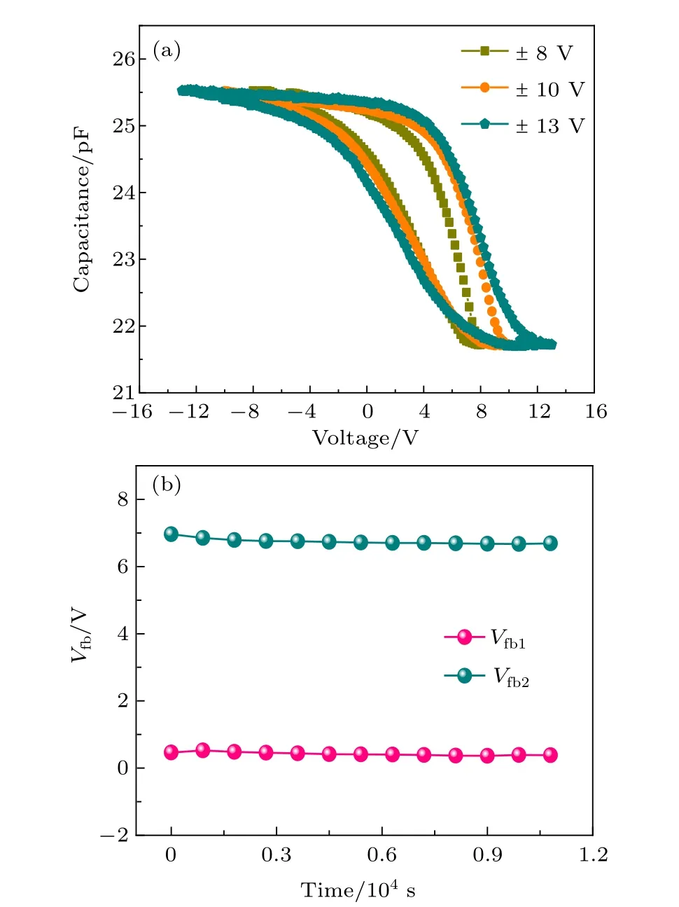
Fig.2.(a)The C–V curves with different scan voltages and(b)the flat band voltage retention of the fabricated sample with 760 ◦C annealing.
In order to in-depth investigate the data retention property,the capacitance retention was also tested for the device annealed at different annealing temperatures. As shown in Fig.3,the high/low state capacitances were tested using a scanning gate voltage of±13 V.The high(or low)capacitance was measured at a fixed voltage of −3 V(or 3 V)every 10 s.Obviously,figure 3(c)shows the optimal retention characteristics.After about 104s of device testing,the degradation of high and low state capacitances is 1%and 1.7%,respectively,indicating great data retention capability of this proposed CTM device.

Fig.3.Long-term retention measurement of the high/low state capacitances for CTM devices annealed at(a)600 ◦C,(b)680 ◦C,(c)760 ◦C,and(d)780 ◦C,respectively.
The CTM device based on the 760◦C annealing has such excellent performance,which is originated from oxygen vacancies and an inter-diffusion layer that improves the charge trapping capability.[9,35]To further confirm the memory mechanism,its microscopic characterization analysis was studied by TEM and XPS in detail. Figures 4(a)–4(d)are the cross-sectional TEM images for the different annealing temperatures,respectively. The TEM figures show that the thickness of the SiO2layer annealed at 600◦C,680◦C,and 780◦C is respectively 2.0 nm,2.4 nm,and 3.3 nm,while the thickness is 3.0 nm for the devices annealed at 760◦C.The thickness of the SiO2tunneling layer is controlled by the annealing temperature,which is a simple and low-cost way to fabricate a series of charge trapping memories with different characteristics.[31,32]Meanwhile,the interface of Ga2O3/SiO2becomes unclear enough,which indicates that there are interdiffusion layers generated with the increase of the annealing temperature.
Figure 5 displays the XPS spectra in various depths from the Ga2O3to SiO2layers of the CTM device annealed at 760◦C.The binding energy peaks of Ga 3d,Ga 2p1/2,and Ga 2p3/2originated from the Ga–O bonding of Ga2O3are respectively centered at 19.5 eV,1143.6 eV,and 1116.8 eV,as shown in Fig.5(a),which is consistent with the report of Kong et al.[33]The diversification of the various Si suboxides with depths at the Ga2O3/SiO2interfaces is obviously reflected in Fig.5(b).[34]Figure 5(c)shows that the peaks of O 1s binding energy are located at 530.1 eV.The peak width of oxygen XPS broadens close to the SiO2layer due to the increase of the lattice oxygen,which demonstrates the presence of oxygen vacancies.[9,35]Atom concentration of Ga,Si,and O elements is counted in the various depths from Ga2O3to SiO2layers as shown in Fig.5(d).The above results show that oxygen vacancies and an inter-diffusion layer are critical for the performance improvement of CTM devices.
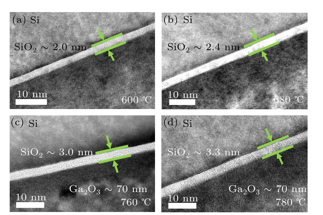
Fig.4. Cross-sectional TEM images of Au/Ga2O3/SiO2/Si structures annealed at(a)600 ◦C,(a)680 ◦C,(a)760 ◦C,and(a)780 ◦C.
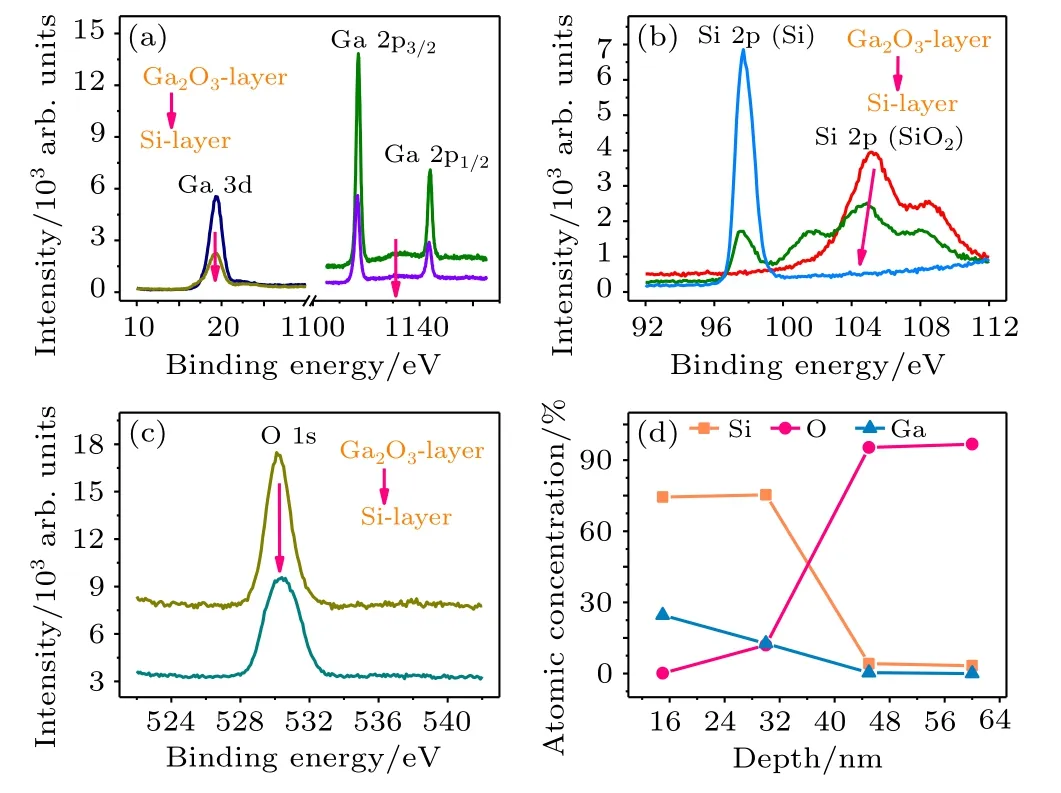
Fig.5.XPS depth analysis of the device annealed at 760 ◦C:(a)Ga 2p3/2,2p1/2,and 3d spectrum,(b)Si 2p spectrum,(c)O 1s spectrum,and(d)atom concentration with various depths from Ga2O3 to Si layers.
4.Conclusion
In summary,we have studied the charge storage and data retention characteristics of the CTM device with an Au/Ga2O3/SiO2/Si structure. The memory storage windows vary with annealing temperatures,and the largest memory window is 6 V resulted from an annealing temperature of 760◦C.At a working voltage range of±13 V,the planar charge trapping density of this CTM device is approximately 7.6×1011cm−2.After about 104s of device testing,the degradation of high and low state capacitances is 1%and 1.7%,respectively. These properties are attributed to the oxygen vacancies and the inter-diffusion layer of Ga2O3and SiO2.This proposed Au/Ga2O3/SiO2/Si structure is promising for the next-generation of CTM devices.
猜你喜欢
凤凰动漫(军事大王)(2022年9期)2022-11-05
凤凰动漫(军事大王)(2022年5期)2022-08-22
凤凰动漫(军事大王)(2022年1期)2022-04-19
小天使·一年级语数英综合(2020年4期)2020-12-16
小天使·一年级语数英综合(2020年5期)2020-12-16
小天使·一年级语数英综合(2020年5期)2020-12-16
作文评点报·低幼版(2020年42期)2020-12-14
造纸信息(2019年7期)2019-09-10
作文大王·低年级(2019年3期)2019-04-19
福建中学数学(2016年8期)2016-12-03

- Chinese Physics B的其它文章
- Compact finite difference schemes for the backward fractional Feynman–Kac equation with fractional substantial derivative*
- Exact solutions of a(2+1)-dimensional extended shallow water wave equation∗
- Lump-type solutions of a generalized Kadomtsev–Petviashvili equation in(3+1)-dimensions∗
- Time evolution of angular momentum coherent state derived by virtue of entangled state representation and a new binomial theorem∗
- Boundary states for entanglement robustness under dephasing and bit flip channels*
- Manipulating transition of a two-component Bose–Einstein condensate with a weak δ-shaped laser∗