
Electronic properties of size-dependent MoTe2/WTe2 heterostructure*
2019-11-06 00:45JingLiu刘婧YaQiangMa马亚强YaWeiDai戴雅薇YangChen陈炀YiLi李依YaNanTang唐亚楠andXianQiDai戴宪起
Chinese Physics B 2019年10期
关键词:马亚
Jing Liu(刘婧),Ya-Qiang Ma(马亚强),†,Ya-Wei Dai(戴雅薇),Yang Chen(陈炀),Yi Li(李依),Ya-Nan Tang(唐亚楠),and Xian-Qi Dai(戴宪起),‡
1College of Physics and Materials Science,Henan Normal University,Xinxiang 453007,China
2Physics Department,The University of Hong Kong,Pokfulam Road,Hong Kong,China
3School of Physics and Electronic Engineering,Zhengzhou Normal University,Zhengzhou 450044,China
Keywords:first-principles calculations,electronic structures,MoTe2/WTe2 superlattice,strain effects
1.Introduction
Heterostructures consisting of dissimilar materials have been the indispensable elements in modern electronics,including spin valve,[1]photovoltaics,[2]field-effect transistor,[3]energy harvester,[4]etc. Looking beyond conventional threedimensional(3D)semiconductors,creating two-dimensional(2D)heterostructures may provide unprecedented opportunities in device processing and engineering.[5,6]The 2D transition metal dichalcogenides(TMDs)[7,8]have received researchers’attention in view of their favourable electronic,optoelectronic,spin and valley hall properties associated with their direct bandgap and spin–orbit coupled electric sheets.[9]Recently,TMDs have been synthesized successfully through liquid or mechanical exfoliation,[10–12]which paved the way for the further application of TMDs-based devices. Abundant building blocks could be provided by the isolated atomic monolayers of different TMDs to construct either van der Waals heterostructure[13]or lateral heterostructures.[14]Both vertical and lateral heterostructures have been successfully achieved by chemical vapor deposition(CVD)and molecular beam epitaxy(MBE)methods.[15–18]Compared with the van der Waals heterostructures,the in-plane heterostructures with edge contacts are assembled seamlessly,which can tune band offset easier,[19]create novel diodes,and enhance rectifying behavior,emission response,and photovoltaic effects.[20]The construction of lateral heterojunctions will enable new devices,such as in-plane transistors and diodes,[5]complementary logic circuits,and photodetectors to be realized.[20]
Previous studies suggested that increasing the number of interfaces by modulating the ratio between{101}and{001}facets could improve the photocatalytic activity at anatase TiO2surfaces and the optimal ratio was determined to be 45:55.[21,22]Like the scenario of lateral heterostructures,it can be supposed that the quantity of the interfaces may affect the photoelectric properties of the LHSs. Besides,the fabrication of 2D lateral heterostructures relies on the substrate choice,indicating that the strain is inevitable in material growth.[23]Recent studies also showed that the 2D LHSs promise to be used in flexible or stretchable electronics,[24]thus marking the strain engineering feasible and valuable.For heterostructures,the abundant dislocations and defects caused by large lattice mismatch between different materials would severely limit their photoelectric performance and device applications.Selecting suitable materials as the building blocks to construct lateral heterostructures is highly desirable. As typical TMD materials,MoTe2and WTe2have several polymorphs,including semiconducting 2H phase,metallic 1T and 1T’phases,[25,26]where 2H–MoTe2and 1T’–WTe2are energetically more favorable under ambient condition.[27]Thus,aroused is the enormous interest in exploring whether the combination of the 2H–MoTe2in stable state and the 2H–WTe2in metastable state can exist stably and results in excellent physicochemical properties. Many efforts have been devoted to 2D TMDs lateral heterostructures in both experiment and theory.The MoTe2-based p–n diodes have been constructed for optoelectronic logics.[28]Gong et al.[29]reported a method of growing the scalable single-step vapour phase for both vertical and in-plane WS2/MoS2heterojunctions.Huang et al.[5]grew the MoSe2/WSe2heterojunctions by lateral heteroepitaxy through using physical vapour transport. Wei et al.[30]investigated the MoS2/WS2and MoSe2/WS2in-plane heterostructures by using first principle calaulations.However,a systematic study of the building block width and strain effect on MoTe2/WTe2lateral heterostructure is still lacking.
Here in this work,stimulated by the past achievements,we investigate the electronic properties of MoTe2/WTe2lateral heterostructures with increased building blocks by using first principle method and also study the efficient band gap engineering through external biaxial strain modulations.Some attractive properties are found,which open the way to exploring the MoTe2/WTe2-based electronics beyond the current scope.
2.Computational methods
The first-principles density functional theory(DFT)[31,32]calculations were employed in conjunction with the projector augmented wave(PAW)[33]scheme as implemented in the Vienna ab initio simulation package(VASP).[34–36]The exchange and correlation contributions were determined by Perdew–Burke–Ernzerhof(PBE)from the generalized gradient approximation(GGA).[37]The cutoff energy for the planewave expansion of wave functions was chosen to be 500 eV and the atomic positions were fully relaxed to an energy convergence of 10−5eV and force convergence of 0.01The K-points-resolved typical value is 0.02 2which is determined by a fine grid of the Monkhorst–Pack method[38]in the Brillouin zone through VASPKIT package.[39]We used the periodic boundary conditions and a vacuum space of 15in the z direction to eliminate the spurious interaction between repeat images.In addition,the spin–orbit coupling(SOC)effect was included in the calculations of self-consistent electronic structure and the band structures were also examined by the Heyd–Scuseria–Ernzerhof(HSE06)hybrid functional[40]for selected lateral heterostructures. Besides,ab initio molecular dynamics(AIMD)simulations were carried out to examine their thermal stability by using the 3×3×1 supercells for A-11 LHS containing 108 atoms and 5×2×1 supercells for Z-11 LHS containing 120 atoms at 300 K in time steps of 1 fs.
3.Results and discussion
As typical TMD materials,monolayer Mo(W)Te2has a hexagonal crystal structure with the Mo(W)layer sandwiched between two Te layers.The in-plane heterostructure superlattice is constructed by stitching MoTe2and WTe2laterally in the same plane. To mimick the interfaces,the rhombic unit cell of MoTe2and WTe2are changed into a rectangular one,so are the Brillouin zones.In our study,there is no obvious lattice mismatch caused by using superlattice models to simulate MoTe2/WTe2heterostructure,which guarantees further experimental epitaxial quality with enhancing the electrical and optical capabilities of the interfaces. The lattice structures of MoTe2/WTe2heterojunctions with the one-dimensional(1D)interfaces along armchair and zigzag edge after geometry relaxation are illustrated in Figs.1(a)and 1(b),respectively.For convenience,the MoTe2/WTe2LHSs are denoted as A-mn for armchair interface while Z-mn for zigzag interface,where the index of m and n refer to the number of MoTe2and WTe2building units,respectively. It can be seen that the building blocks are seamlessly stitched together with almost no distortion being found along interlines.The interface boundaries in all considered MoTe2/WTe2LHSs remain distinguishable and sharp after geometry relaxations.

Fig. 1. Top and side view atomic configurations of (a) A-mn MoTe2/WTe2 LHS and(b)Z-mn MoTe2/WTe2 LHS.
After constructing various MoTe2/WTe2LHSs,the priority is to confirm their stability and assess the feasibility experimentally.The binding energy of the lateral heterostructure,as the energy gain in assembling MoTe2/WTe2LHSs,is calculated from the following equation:

where Etotis the energy of the constructed LHSs,EMoTe2and EWTe2are,respectively,the total energy of MoTe2and WTe2component relative to that of their corresponding monolayer structures.The calculated Ebvalue is −13 meV for A-11 LHS and −5 meV for Z-11 LHS.As m and n increase from 1 to 6,the binding energy shows negligible difference and tends to be convergent.It is noteworthy that the decisive factor affecting the stability of LHS is related to the number of the interfaces between different building blocks.Accordingly,it is significant to study the structural stability of A-11 and Z-11 LHSs which own the maximum number of interfaces with serial building units.Then,the thermal stability of the A-11 and Z-11 LHSs are examined by ab initio molecular dynamics simulations.The variation of total energy and temperature during the simulation time as well as the snapshots of atomic configurations are shown in Fig.2.After heating at 300 K for 6 ps,neither broken bonds nor obvious structure distortion is found in the contact,and the oscillation for total energy is relatively slight during the AIMD simulation,[41]which confirms the fabrication of such LHS could be thermodynamically feasible in practice.

Fig.2. Variation of total energy and snapshot structures with time of(a)A-11 and(b)Z-11 LHSs in the molecules dynamic simulation at 300 K in time steps of 6 ps.
To study the electronic properties of these lateral heterostructures,the projected band structures at their optimized structured are calculated next. The band structure and corresponding atomic configurations of the pristine MoTe2and WTe2monolayers are presented in Figs.3(a)and 3(b).Both the relaxed MoTe2and WTe2building blocks have a rectangular lattice with size of a=3.55 ˚A and b=6.15The obtained bond length of Mo–Te and W–Te are 2.73and 2.74respectively. The direct semiconducting character is observed in either MoTe2or WTe2monolayer with the bandgap value of 1.08 eV and 1.06 eV,respectively,which are corresponding to previous results.[42]Considering that the Mo and W atoms may have strong intrinsic SOC effect,taking the A-11 and Z-11 LHSs for example,the band structures of these two LHSs with and without the SOC effect are calculated as shown in Figs.3(c)–3(f).The A-11 and Z-11 LHSs also show the direct band gap semiconductor character and the band gap is located at P-point,which is sited on 1/3 X–Γ(the Q-point that will be sited on 0.24 X–Γ and mentioned later)in the rectangular Brillouin zone.The nonmagnetic nature is also maintained in both A-11 and Z-11 MoTe2/WTe2LHSs,which can be ascribed to the formation of perfect interfaces between different building blocks without any dangling bonds to sustain the pristine coordination numbers.Additionally,the dots in the band structures with different colors and diameters mean the orbital contributions from opposite MoTe2and WTe2components.The two kinds of building units with continuous spatial distribution lead to the mixed orbitals from both building blocks in the VBM and CBM.Based on the PBE method,the band gap value is 1.08 eV for A-11 LHS and the VBM and CBM move down to the lower energy in comparison with MoTe2monolayer while move up to the higher energy in comparison with WTe2monolayer.The band gap value is 1.05 eV for Z-11 LHS with the VBM and CBM shift towards the high energy level compared to both MoTe2and WTe2monolayers.As the SOC effect is considered,the energy splitting caused by the lack of inversion symmetry in 2H–TMDs narrows the band gap in both A-11 LHS and Z-11 LHSs.By contrast,the SOC effect applied on A-11 and Z-11 LHSs have no material influence on orbital contributions that origin from MoTe2and WTe2building blocks. Moreover,the projected band structure of A-11 and Z-11 LHSs with SOC effect also confirm the direct-gap semiconducting character. In order to verify the results predicted above,the calculated band structure of A-11 LHS and Z-11 LHS based on HSE06 level are provided in Fig.4. It can be seen that the energy gaps are still located at the P-point with the direct gap semiconducting character and the band gap value is,separately,1.51 eV for A-11 LHS and 1.47 eV for Z-11 LHS.The difference is minimal except for the changed bandgap values.Therefore,the DFT-PBE theory without SOC effect is reliable in describing such a kind of MoTe2/WTe2LHS and the PBE method without SOC will be adopted in the following studies.

Fig.3.Band structures of pristine(a)MoTe2 and(b)WTe2 monolayers,where black dashed rectangles present the building blocks of the LHSs.Projected band structures of A-11 LHS(c)without and(d)with SOC effect.Projected band structures of Z-11 LHS(e)without and(f)with SOC effect.Orange and red dots represent MoTe2 units,and green and blue dots refer to WTe2 units.The band gaps are marked by blue arrows.

Fig.4.Band structures of(a)A-11 LHS and(b)Z-11 LHS based on HSE06,with blue arrows indicating bandgaps and horizontal solid lines representing Fermi level.
To investigate the MoTe2/WTe2LHS comprehensively,the electronic properties of A-mn and Z-mn(m=n=2,3,4,5,6)lateral heterostructures are further studied,respectively. The corresponding projected band structures of the LHSs with armchair interface are illustrated in Figs.5(a)–5(e)while those of the LHSs with zigzag interface are shown in Figs.5(f)–5(j).A common feature is that the VBM and CBM are contributed by opposite components,manifesting the type-II band alignment.What is more,the feature becomes more obvious with the width increasing because of the wider spatial distributions of different building blocks.A similar phenomenon was also observed in the lateral heterostructure of arsenene and antimonene.[43]The chemical potential difference between MoTe2and WTe2building blocks causes the band to be bent at the contact,which causes the photon-generated electron–hole pairs to be separated at opposite domains[44]in MoTe2/WTe2LHS.Type-II band alignment occurring in the MoTe2/WTe2LHS is efficient to facilitate the quantum efficiency and can make MoTe2/WTe2LHS a appealing candidate for solar cells.Similarly,the out-of-plane MoTe2/WTe2heterostructure also shows the type-II alignment.[45]Meanwhile,the direct band gap character remains in all considered LHSs and the gap changes in range of 0.01 eV.However,the position of CBM and VBM shift from P-point to Γ-point in A-33 and A-66 LHSs. To further study the variation of band gap location,we put emphasis on the A-mn LHSs with different ratios of building blocks in the following. From Table 1,it can be found that the bandgap location can change from Ppoint to Γ-point when m plus n is a multiple of 3.As a result of Brillouin zone folding,P-point can be folded to Γ-point in the Brillouin zone when expanding to a triploid supercell for A-mn superlattice structure.For Z-mn LHSs,Brillouin zone folding occurs in Γ–Y and A–X,which has noinfluence on the bandgap location.In fact,the bandgap located at the high symmetry Γ-point rather than at the arbitrary point in the X–Γ is beneficial to optoelectronic device because of the convenient electron transition. It is noteworthy that the direct bandgap semiconducting nature also remains in all considered LHSs.

Table 1.Bandgap locations of all considered A-mn LHSs,with m and n denoting the number of MoTe2 and WTe2 building blocks,respectively.Solid circle and empty circle represent bandgaps located at Γ and P points,respectively.
Unlike 2D vertical heterostructures,the building blocks in the in-plane heterostrutures are connected by chemical bonding other than stacked by vdW interactions due to the distinct and clean interlines.In order to validate the bonding properties within the interfaces,taking A-55 and Z-55 LHSs for example,the corresponding plane-integrated and the 3D isosurface of charge density difference are demonstrated in Figs.6(a)and 6(b). The charge redistribution mainly exists near the interlines and the electrons flow from WTe2to MoTe2,which will produce a build-in electric field and cause the band to be bent near the interface,which is favorable for the efficient separation of photogenic charges.[46]Besides,the significant charge transfer around the grain boundaries suggests the strong ionic bonds in the LHS.To further confirm the bonding character,the electron localization function(ELF)of the Mo–Te and W–Te bonds away from and across the interlines are shown in Figs.6(c)and 6(d),respectively. Unlike the As/Sb LHS and some other lateral heterostructures,the Mo–Te and W–Te bonds across the interface show the typical ionic bonding,for the substantial concentration of electrons is only localized around Te atoms.By comparison,the ELF of Mo–Te and W–Te bonds that are away from the interface is very similar to the above case.The results also indicate the feasibility in synthesizing the MoTe2/WTe2LHS.
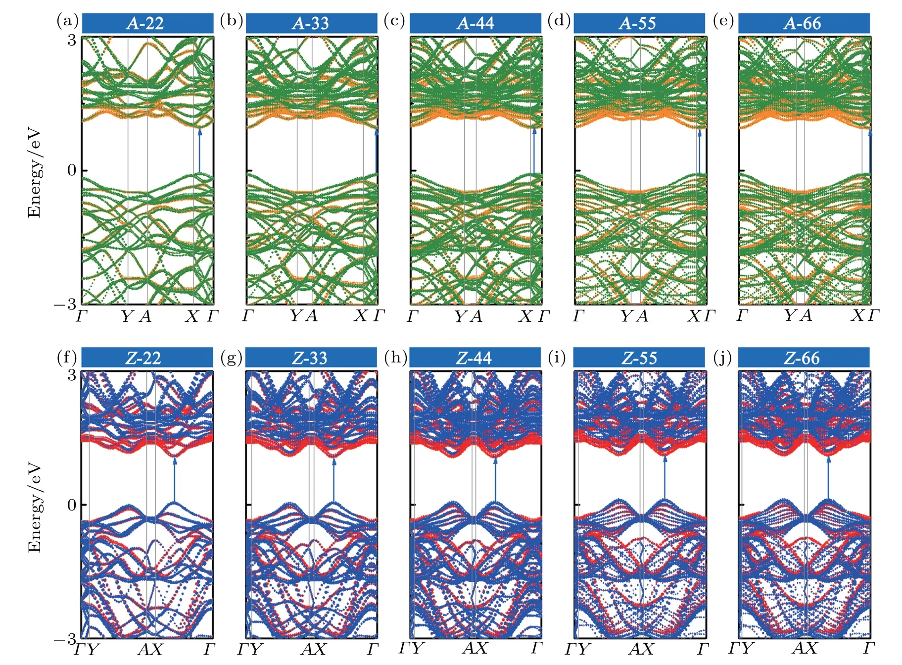
Fig.5.Projected band structures of(a)A-22,(b)A-33,(c)A-44,(d)A-55,(e)A-66,(f)Z-22,(g)Z-33,(h)Z-44,(i)Z-55,and(j)Z-66 LHSs,respectively.
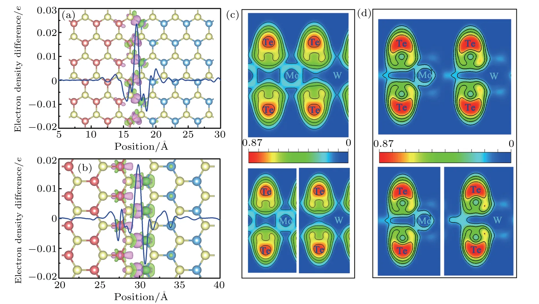
Fig.6.Plane-integrated electron density difference and 3D isosurface of electron density difference(background)of(a)A-55 LHS and(b)Z-55 LHS,where purple and green areas represent electron accumulation and depletion,respectively,and isosurface value is set to be 0.005 Electron localization function(ELF)of Mo–Te and W–Te bonds across(upper)and away from(lower)interlines for(c)A-55 LHS and(d)Z-55 LHS,respectively.
To study the variations of electronic structure near the interfaces,the local density of states(LDOS)projected on Mo(W)and two Te atoms adjacent next to the contacts of A-55 and Z-55 LHSs are plotted in Fig.7.The interfaces can be easily distinguished from the electronic structures.For A-55 LHS as shown in Figs.7(a)–7(f),the CBM and VBM state shift towards low energy compared with the pristine MoTe2unit cell.When approaching to interline,the first peak in unoccupied state becomes smaller and the occupied states move towards the Fermi level,leading the bandgap value to decrease. As shown in Figs.7(g)–7(l),the CBM states shift towards low energy while the VBM states shift towards the Fermi energy compared with intrinsic WTe2unit cell.The unoccupied states move towards the Fermi energy,reducing the bandgap value with approaching to the interface.The LDOS on Mo(W)and Te atoms of Z-55 LHS show a similar tendency of A-55 LHS.It can be seen clearly that the band bending occurs near the 1D interface,which consists with previous analysis.

Fig.7.(a),(a′))Total density of states(TDOS)of pristine MoTe2 unit cell,(l),(l′)total density of states(TDOS)of pristine WTe2 unit cell,and(a)–(k),(a′)–(k′)local density of states(LDOS)of Mo(W)and Te atoms(between the two black dashed lines)adjacent to the interface region corresponding to A-55 LHS(top panel)and Z-55 LHS(bottom panel).
For applications in nanodevices,bandgap engineering is considered as a powerful technique.Previous theoretical investigations reveal that an external strain has a remarkable influence on the band structure and dielectric constant of twodimension semiconducting TMDs.[47,48]In addition,applying suitable biaxial strain is an effective way to manipulate the electronic properties of MoTe2-based alloy compound.[49]The 1D interfaces formed by MoTe2and WTe2are strain free due to the negligible lattice mismatch.Therefore,taking the A-22 and Z-22 LHSs for example,an external biaxial strain is used to manipulate the band structures of MoTe2/WTe2lateral heterostructures.The biaxial strain effects on band edge variation for A-22 and Z-22 LHSs are calculated in Figs.8(c)and 8(d),respectively.The in-plane strain is defined as ε=(c−c0)/c0,where c0and c refer to the lattice constant of unstrained and strained supercell,respectively.For brevity,−ε represents the compressive strain.As shown in Fig.8(c),the band-gap of A-22 LHS retains direct and decreases gradually as tensile strain increases. The band gap transition dependent on the expansile lattice constant is linear and monotonic. On the other hand,as the compressive strain increases,the value of band gap initially increases until ε=−2%and then decreases continually to a strain of −4%. There is also a direct–indirect transition at a critical strain of −2%.The band gap variation tendency dependent on the shrinking lattice is not linear nor monotonic due to the direct–indirect transition.It can be seen from Fig.8(c)that the energy of the lowest unoccupied state at P-point(CBM at P)is lower than that at X-point(CBM at X)under the biaxial tensile strain or a relatively small compressive strain. However,CBM at P moves up until above the CBM at X when the lattice constant is reduced by 1.5%,which causes the direct–indirect transition.Figure 8(d)shows the band edge energy transition of Z-22 LHS.Comparing with the A-22 LHS,the difference is that the CBM state transition is between P and Q points instead of P and X points. Besides,as the compressive strain increases,the value of band gap initially increases until ε=−3%and then decreases to the strain of −4%.As a consequence,the applied external biaxial strain has a remarkable influence on the electronic structures of MoTe2/WTe2lateral heterostructure.To study why the band edge states change with the elastic strain,the TDOS of A-22 and Z-22 LHSs and projected density of states(PDOS)of Mo,W,and Te atoms which are selected around the interfaces are calculated and exhibited in Figs.8(a)and 8(b),respectively.The electronic structures of VBM and CBM in the two LHSs are mainly dominated by Mo-d orbital,W-d orbital and a little by Te-p orbital. The Mo-d and W-d states overlap with the Te-p state significantly,which demonstrates the strong bonding at the interface.When applying a tensile(compressive)strain,the coupling between metal d and nonmetal p orbitals will weaken(strengthen),which further influences the bonding component in the VBM and CBM states and leads to the direct–indirect transition of the band gap.Besides,no band alignment transition is observed after applying the biaxial strain,indicating that the MoTe2/WTe2LHSs can be the candidate materials for the applications in flexible electronics.

Fig.8.Plots of total density of states(TDOSs)and projected density of states(PDOSs)versus energy of(a)A-22 LHS and(b)Z-22 LHS.Fermi energy is set to be zero and indicated by vertical dotted black line.(c)Plots of calculated shift of the band edge energy(VBM states at P and X points,CBM states at P and X points)versus biaxial strain for A-22 LHS and(d)plots of band edge energy(VBM states at P and Q points,CBM states at P and Q points)versus axial strain for Z-22 LHS.
4.Conclusions
Using first-principles methods,we systematically investigate the electronic properties of size-dependent in-plane heterostructures constructed by MoTe2and WTe2building blocks. The corresponding geometric structures are studied and the ab initio molecular dynamics confirms their thermal stability at room temperature. The formed interfaces in all considered MoTe2/WTe2LHSs remain distinguishable and sharp after structure optimization,indicating the feasibility of synthesizing such LHSs. The direct bandgap nonmagnetic semiconductor nature is also observed in both kinds of seamless MoTe2/WTe2LHSs,which can be ascribed to the formation of perfect interfaces between MoTe2and WTe2building blocks. On account of Brillouin zone folding,the band gap location will change from P-point to Γ-point when expanding to a triploid supercell for A-mn LHSs,which is convenient for electron excitation so that these materials may be used in optoelectronic devices.The highly coveted type-II alignment with the physical separation of excitons is also identified,showing the enhanced quantum efficiency and the appealing applications in solar cells,electronics,and photocatalysis.Moreover,the external biaxial strain can lead to efficient bandgap engineering due to the change of nonmetal–metal coupling strength caused by the tensile or compressive strain while no band alignment transitions are observed under different biaxial strains.In general,this research points out a new perspective on electronic and optoelectronic devices and sheds light on exciting new opportunities in material science.
Acknowledgment
The authors thank the High Performance Computing Center of Henan Normal University for computing.
猜你喜欢
中学生数理化·高一版(2022年4期)2022-05-09
思维与智慧·上半月(2022年4期)2022-04-08
中国棉花(2021年5期)2021-01-02
东坡赤壁诗词(2020年3期)2020-07-04
软件(2020年3期)2020-04-20
中学生理科应试(2019年3期)2019-07-08
理科考试研究·初中(2017年4期)2017-11-04
中学生数理化·高二版(2017年3期)2017-07-07
中学生数理化·中考版(2016年10期)2016-12-22
中学生数理化·高二版(2016年9期)2016-05-14

- Chinese Physics B的其它文章
- Compact finite difference schemes for the backward fractional Feynman–Kac equation with fractional substantial derivative*
- Exact solutions of a(2+1)-dimensional extended shallow water wave equation∗
- Lump-type solutions of a generalized Kadomtsev–Petviashvili equation in(3+1)-dimensions∗
- Time evolution of angular momentum coherent state derived by virtue of entangled state representation and a new binomial theorem∗
- Boundary states for entanglement robustness under dephasing and bit flip channels*
- Manipulating transition of a two-component Bose–Einstein condensate with a weak δ-shaped laser∗