
Optical response of an inverted InAs/GaSb quantum well in an in-plane magnetic field∗
2019-11-06 00:46XiaoguangWu吴晓光
Chinese Physics B 2019年10期
Xiaoguang Wu(吴晓光)
1State Key Laboratory for Superlattices and Microstructures,Institute of Semiconductors,Chinese Academy of Sciences,Beijing 100083,China
2College of Materials Science and Opto-Electronic Technology,University of Chinese Academy of Sciences,Beijing 100049,China
Keywords:quantum well,magnetic field,de-polarization effect
1.Introduction
The InAs/GaSb system has been extensive studied for many years,both experimentally and theoretically.It has important technological applications.In recent years,InAs/GaSb short periodic superlattices are used to make highly efficient infrared photo-detectors and detector arrays.[1–3]
On the fundamental research side,the InAs/GaSb quantum well structures have been investigated more extensively,mainly due to its interesting band alignment,i.e.,the so-called broken-gap band alignment.[4–35]In the transport measurements,the edge transport was reported in connection with the two-dimensional topological insulator phase and the quantum spin Hall effect. More recently,the edge transport was also reported in the topologically trivial regime.The new experimental results indicate that,one may have parallel conducting edge channels.This puts a hurdle on the further experimental investigation of the helical edge transport in the InAs/GaSb quantum well system,also on the future quantum device applications.[19–35]
Many optical experiments have also been carried out in the InAs/GaSb quantum well systems.[4–18]In the earlier experiments,the quantum well had a high electron density.In recent years,as the material growth technology progresses,the sample quality increases greatly.Furthermore,as the device processing technology advances,the electron density can nowadays be controlled to the desired value by the back-gating and front-gating techniques.This enables one to explore many interesting properties of the InAs/GaSb quantum well system.In the optical experiments,a perpendicular or a tilted magnetic field was often employed.In some experiments,the measured data can be explained well by the one-electron theory.In some other experiments,however,the explanation of the experimental result needs the inclusion of many-particle effects.In a recent optical transmission experiment,the exciton insulator picture was used to interpret quantitatively the experimental findings. The involved theoretical model is a Coulomb-coupled electron–hole system with no spin–orbit interaction. On the other hand,in the InAs/GaSb quantum well system,especially in the exploration of the helical edge transport in the topological non-trivial phase,the spin–orbit interaction is argued to be a necessary ingredient,and was also found experimentally to be quite important.[4–35]This suggests that,more experimental and theoretical studies are required to further improve our understanding about the electronic structure of the InAs/GaSb quantum well systems.
In an inverted InAs/GaSb quantum well system,the coupling between the InAs layer and GaSb layer will produce a hybridization gap.The existence of the hybridization gap has been explored and confirmed in various experiments.[4–35]For those electronic states around the hybridization gap,the spatial dependence of the corresponding wave functions shows that the electrons and holes reside in different layers.An optical transition across the hybridization gap will involve an electron in the lower energy band in one layer to be excited into the higher energy band in a different layer.This situation is quite similar to the inter-subband excitation in a conventional GaAs quantum well.[36]Because of the spatial separation of the electrons and holes,a dynamical polarization in the growth direction of the quantum well can be induced by the optical excitation.The electron–electron interaction in the quantum well in turn affects the optical response.This is the de-polarization effect.In the conventional GaAs quantum well system,with zero external magnetic field,the dynamical polarization can only be generated by the optical field whose electric field component is non-zero in the growth direction of the quantum well.While in the InAs/GaSb quantum well system,the optical transition matrix element will be non-zero,even when the electric field component is in the quantum well plane.The induced dynamical polarization will become important when the in-plane symmetry of the quantum well is further broken.This can be achieved by applying an in-plane magnetic field.
In this paper,we will study theoretically the optical response of an inverted InAs/GaSb quantum well,in the presence of an externally applied in-plane magnetic field.In the case of a perpendicular magnetic field,or of a tilted magnetic field,the magneto–optical properties of the InAs/GaSb quantum well have been investigated,both experimentally and theoretically.[4–18,37–41]There were also some theoretical study on the transport property of the InAs/GaSb quantum well in the presence of an in-plane magnetic field based on a generalized or extended two-dimensional topological insulator model.[42–44]Our theoretical result shows that,as the strength of the in-plane magnetic field increases,the de-polarization effect originated from the electron–electron interaction in the InAs/GaSb quantum well becomes more important,and the in-plane optical response of the quantum well becomes asymmetrical. It is hoped that some experimental studies will be reported in future so that a more detailed comparison can be made.
This paper is organized as follows:In Section 2,the theoretical formulation is briefly presented. Section 3 contains our calculated results and their discussions.Finally,in the last section,a summary is provided.
2.Formulation and calculation
The InAs/GaSb quantum well studied in this paper is a[001]grown quantum well,embedded in the AlSb barriers.The single-particle electronic structure is calculated within the 14-band κ·ρ approximation.[45–51]The parameters for the constituting materials used in the calculation are widely used by others.The 14-band model can reproduce the experimental values for the bulk conduction band effective mass,the hole band mass,and the conduction band g-factor. The 14-band model is chosen because the 8-band model fails to produce reliable electronic states,when one considers a high index grown InAs quantum well.The spin–orbit interaction,the effect of strain,and the influence due to the non-common-atom interface correction are taken into account.The quantum well is in the xy plane,with the x axis along the[100]direction,the y axis along the[010]direction.The growth direction of the quantum well[001]is taken as the z axis.The in-plane magnetic field is taken into account by considering the vector potential(Byz,−Bxz,0)which generates the in-plane magnetic field(Bx,By,0).
In the calculation of the optical response of the InAs/GaSb quantum well,the self-consistent linear response approach is used.[36,52–54]We wish to point out that the selfconsistent linear response method utilized in the present work is quite similar to that described in the paper of Ando,Fowler,and Stern.[36]Thus,the formulations will not be repeated here,and only a brief description will be given. The total system Hamiltonian can be written as H=H0+Hex+Hin.H0describes the 14-band model plus the in-plane magnetic field,Hexis due to the external optical field,and Hindescribes the frequency-dependent potential generated by the dynamical polarization which is induced by the external optical field. The self-consistent condition is such that,the induced potential Hinis generated by the total perturbation Hex+Hin. Thus,within the linear response approximation,one has Hin=F(Hex+Hin),with F a linear functional.

Once the induced charge density is obtained selfconsistently,one can calculate the optical response of the system,δvα=F1(Hex+Hin),the correction to the averaged value of the velocity operator vαdue to the total perturbation field.Within the linear response approach,one has another linear functional F1.In the above equation,the subscript α denotes the direction of the velocity,one has α=x,y.In the conventional linear response approach,one only considers the correction due to the external field.In this case,the optical response is characterized by the velocity–velocity correlation function,or the current–current correlation function,typically denoted as σα,β(ω),which is proportional to the frequency dependent dynamical conductivity.[52,53]Note that,one may consider the many-particle effect due to the electron–electron interaction at this stage,but,the many-particle effect here does not include the de-polarization effect.Note also that,when the velocity–velocity correlation function is approximately calculated for the non-interacting fermion system,the frequency dependence of the correlation function can reflect the energy difference between different bands involved in the optical transition.[52–54]In our self-consistent linear response approach,one still has δvα(ω),a frequency-dependent velocity correction.In general,it is not given by the conventional velocity–velocity correlation function,but is given by a bi-linear functional of two velocity operators.Without any confusion,we will still denote the correction δvα(ω)as σα,β(ω),with β denotes the direction of the electric field in the externally applied optical field.In this paper,the unit of velocity is(meeV/2)1/2.Note also that,the frequency ω above is the frequency of the externally incident optical field.
3.Results and discussions
In this section,we present our numerically calculated optical response for a specific InAs/GaSb quantum well. The considered quantum well has the InAs layer width 12.5 nm,and the width of the GaSb layer is 5 nm.This is an inverted InAs/GaSb quantum well.The in-plane magnetic field is assumed to be along the y axis.One may take the in-plane magnetic field in an arbitrary in-plane direction,but the singleparticle electronic states of interest are found to only show a very weak directional dependence. Therefore,the above choice is a reasonable one. In the calculation of the singleparticle electronic states,the transferring of electrons between the InAs layer and the GaSb layer is not allowed. In doing so,the change of the electronic states due to the in-plane magnetic field can be more clearly identified. The fermi energy required in the calculation of the optical response is also fixed at the zero in-plane magnetic field value. This is a reasonable assumption,because in an experiment,the fermi energy is controlled externally by the front-gate and back-gate bias voltages.In our calculation,when the in-plane magnetic field is zero,the fermi energy is assumed to be in the hybridization gap.It should be pointed out that,a rather dense/fine mesh,typically 200×200,is needed in the calculation of the electronic states in the wave vector space.Therefore,the numerical calculation presented in this paper requires a large computational resource.
In Fig. 1, the velocity–velocity correlation function σyy(ω)is plotted versus the frequency ω for different values of the in-plane magnetic field strength:in the panel(a)By=0 T,in the panel(b)By=2 T,in the panel(c)By=4 T,and in the panel(d)By=6 T.The correlation function is in general a complex function of the frequency.The real part is plotted as the black solid curve,and the imaginary part is plotted as the red dashed curve.In Fig.1,the direction of the electric field in the incident light is along the y axis,the same direction as the in-plane magnetic field.In this case,the induced dynamical charge density p is negligibly small,therefore the de-polarization effect is practically zero.The correlation function shown in the Fig.1 is obtained by treating the system as non-interacting fermions with a line broadening inserted.In the long wave length limit,this should be a good approximation as there is no intra-band single-particle excitation.[36]It also should be pointed out that the optical response σyy(ω)satisfies the conventional Kramers–Kronig relation.[52,53]

Fig.1.The velocity–velocity correlation function σyy(ω)versus the incident light frequency ω for different values of the in-plane magnetic field strength:(a)By=0 T,(b)By=2 T,(c)By=4 T,and(d)By=6 T.The real part is plotted as the black solid curve,and the imaginary part is plotted as the red dashed curve.
One can see that,at By=0,as shown in Fig.1(a),the imaginary part of σyy(ω)shows two dips. The frequencies corresponding to these two dips can be identified as the transition energies around the hybridization gap by examining the calculated band structure.[41]The transitions at the lower frequency dip and at the higher frequency dip are the transitions between energy bands with different spins.This clearly shows that the spin–orbit interaction in InAs/GaSb quantum wells is quite strong as expected.As the strength of the in-plane magnetic field increases,one observes in Fig.1(see panels(b),(c),and(d))that,the imaginary part of σyy(ω)still shows a twodip structure,and the position of two dips in the imaginary part of σyy(ω)is almost not shifted.The width of the dips becomes broadened as the in-plane magnetic field becomes larger. It should be pointed out that,as the in-plane magnetic field increases to By=6 T(Fig.1(d)),the band structure has been modified drastically.The system is no longer gapped anymore.At By=0,the system is a gapped semiconductor,while at By=6 T,the system becomes a non-gapped semi-metal.However,the main features in the imaginary part of σyy(ω)largely remains unchanged.This is because that,the optical response is determined not only by the energy band structure but also by the optical transition matrix elements over the entire wave vector space.The hybridization nature in the InAs/GaSb quantum well between the conduction band of the InAs layer and the valence band of the GaSb layer still exists in the presence of the in-plane magnetic field.It should be pointed out that,the size of the hybridization gap at zero in-plane magnetic field can be affected by the doping and by the gate bias.[4–35]
In Fig. 2, the velocity–velocity correlation function σxx(ω)is shown versus the frequency ω for different values of the in-plane magnetic field strength:(a)By=0 T,(b)By=2 T,(c)By=4 T,and(d)By=6 T.The real part is plotted as the black solid curve,and the imaginary part is plotted as the red dashed curve.In Fig.2,the direction of the electric field of incident light is along the x axis perpendicular to the in-plane magnetic field.The motion of the electrons driven by the electric field will be affected by the lorentz force induced by the in-plane magnetic field.In this case,the de-polarization effect has to be taken into account.It should be pointed out that,the optical response σxx(ω)will satisfy a generalized Kramers–Kroning relation,but not the conventional Kramers–Kroning relation which directly relates the real part and the imaginary part of the response function.[52,53]There exists a kernel function from which the real part and the imaginary part of the optical response function can be generated.
At zero magnetic field,as shown in Fig.2(a),the dynamical polarization is negligibly small because the contribution from different optical transitions at various wave vectors largely cancels out each other.In this case,σxx(ω)is practically the same as σyy(ω).The InAs/GaSb quantum well system considered here has a structure inversion asymmetry,thus they are slightly different.Like σyy(ω)shown in Fig.1,the imaginary part of σxx(ω)also shows two dips.As the in-plane magnetic field increases,one observes that the dip at lower frequency is not shifted,but the dip at higher frequency shifts towards the high frequency direction. The dip structure becomes weaker as the in-plane magnetic field increases.When the in-plane magnetic field reaches By=6 T,the two-dip feature cannot be seen anymore. This is expected. Just as the name of de-polarization effect implies,the de-polarization effect will depress those resonant contributions to the optical response that produce the dynamical polarization.[36]Thus,the in-plane optical response of the InAs/GaSb quantum well system becomes asymmetrical(σxx(ω)σyy(ω))due to the inplane magnetic field.

Fig.2. The velocity–velocity correlation function σxx(ω)versus the frequency ω for different values of the in-plane magnetic field: (a)By=0 T,(b)By=2 T,(c)By=4 T,and(d)By=6 T.The real part is plotted as the black solid curve,and the imaginary part is plotted as the red dashed curve.The de-polarization effect is taken into account.
It should be pointed out that,there exists another in-plane optical asymmetry. The optical response function σxy(ω)is not zero(not shown in this paper). Both the real part and the imaginary part of σxy(ω)display an oscillatory behavior versus the frequency ω.Its magnitude is about tenth of σxx(ω)or σyy(ω).σxy(ω)is not zero because the InAs/GaSb quantum well system studied in the present paper has a structureinversion asymmetry.This asymmetry is known to induce a large Rashba-type spin–orbit coupling and a non-zero σxy(ω).For a symmetrical quantum well made of narrow band gap semiconductors,like InAs or InSb,one can verify that σxy(ω)will vanish.
In order to see the de-polarization effect more clearly,in Fig.3,the velocity–velocity correlation function σxx(ω)is also plotted versus the frequency ω for different values of the in-plane magnetic field strength:in panel(a)By=0 T,in panel(b)By=2 T,in panel(c)By=4 T,and in panel(d)By=6 T.But,in Fig.3,the de-polarization effect is removed. Note that,the screening effect,that arises also from the electron–electron interaction,should reduce the de-polarization effect somewhat.This screening effect has not been considered in the present study,as the numerical work will be much more involved. In Fig.3,the real part of σxx(ω)is plotted as the black solid curve,and the imaginary part is plotted as the red dashed curve.

Fig.3. The velocity–velocity correlation function σxx(ω)versus the frequency ω for different values of the in-plane magnetic field: (a)By=0 T,(b)By=2 T,(c)By=4 T,and(d)By=6 T.The real part is plotted as the black solid curve,and the imaginary part is plotted as the red dashed curve.The de-polarization effect is not included.
By comparing Fig.2 and Fig.3,the difference is obvious.When the de-polarization effect is absent,the imaginary part of the optical response function,σxx(ω),shows a two-dip structure as the function of the frequency ω,and this feature persists up to By=4 T.At By=6 T,the dip at lower frequency becomes weak,but the dip at higher frequency can still be clearly identified.One also observes that,the position of the dip at lower frequency does not change as the in-plane magnetic field increases.The position of the dip at higher frequency shifts towards the low frequency direction.The above dependence on the in-plane magnetic shown in Fig.3 is also different from that shown in Fig.1. As one would expect,the in-plane magnetic field introduces an in-plane asymmetry.One may explore this controllable symmetry breaking to obtain more information about the electronic property of the InAs/GaSb quantum well systems.
In the calculation of the optical response of the InAs/GaSb quantum well system,one needs the energy levels and the corresponding wave functions for each point in the wave vector space. Let us examine this in more detail.When the de-polarization effect is ignored,the optical response is characterized by the velocity–velocity correlation function σα,β(ω). This correlation function can be written down easily when one approximately treats the system as noninteracting fermions.One would obtain

with nFthe Fermi distribution function.Note that the correlation function σα,β(ω)given above is slightly different,within a numerical factor,from the usual dynamical conductivity displayed in the textbook.[52,53]It is clear that one needs to perform a sum over the band indexes n1and n2,and a sum over κ the wave vector.Thus,the correlation function above can be viewed as an integral of a frequency-dependent energy resonant term(given by the second line in the above equation)weighted by the optical transition matrix elements.
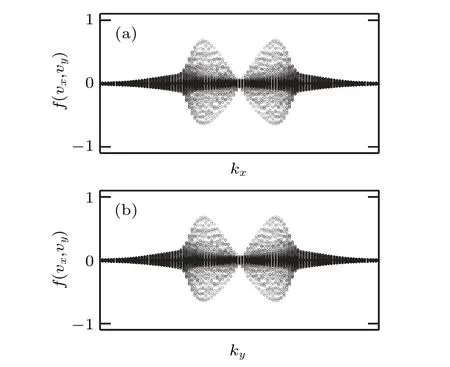
Fig.4. The distribution of velocity matrix elements f(vx,vy)=on the(kx,ky)plane. The in-plane magnetic field is zero.(a)View the distribution versus the kx.(b)View the distribution versus the ky.The index n1 takes the value of two bands below the hybridization gap,and the index n2 takes the value of two bands above the hybridization gap.
The in-plane magnetic field will modify the band structuredrastically. However,it is believed that the topology of the electronic states will remain non-trivial,even for a rather strong in-plane magnetic field.Therefore,it is interesting to examine the overall structure of the distribution of the optical transition matrix elements.In Fig.4,the distribution of velocity matrix elements f(vx,vy)defined as f(vx,vy)=on the(kx,ky)plane is displayed in the case of zero in-plane magnetic field.The imaginary part of f(vx,vy)is almost zero. Therefore,only the real part of f(vx,vy)is shown in Fig.4. In panel(a),the distribution is viewed along the kxaxis for all values of ky. Each value of f(vx,vy)is plotted as a small solid dot.In panel(b),the distribution is viewed along the kyaxis,for all values of kx.The matrix element characterizes the strength of the optical transition between two bands specified by the band index n1and n2.In Fig.4,the index n1takes the value of two bands below the hybridization gap,and the index n2takes the value of two bands above the hybridization gap.From Fig.4,one observes that,the global structure of the distribution of the optical transition matrix element looks like two head-to-head tadpoles,in both panel(a)and panel(b).We may call this a two-tadpole topology in the wave vector space.
In Fig.5,the distribution of velocity matrix elementson the(kx,ky)plane is displayed for the case of a non-zero in-plane magnetic field By=6 T.The imaginary part is almost zero.Only the real part is shown.In panel(c),the distribution is viewed along the kxaxis.In panel(d),the distribution is viewed along the kyaxis.The band indexes n1and n2take the same values as those in Fig.4.One observes that,the same two-tadpole topology remains.The distribution of f(vx,vy)is examined for other values of the in-plane magnetic field(By<6 T),and it is found that the two-tadpole topology remains.Similarly,one can examine the distribution of other optical transition matrix elements,for example,f(vx,vx)and f(vy,vy),defined in ways similar to the above definition of f(vx,vy). It is found that,f(vx,vx)and f(vy,vy)have the same topology at zero in-plane magnetic field.This is expected.Furthermore,the topology remains the same when the in-plane magnetic field increases from zero up to a moderate value. It should be pointed out that,the velocity matrix elements f(vx,vy)take positive and negative values.Because of this,the magnitude of σxy(ω)is smaller than that of σxx(ω)and σyy(ω).

Fig.5. The distribution of velocity matrix elements f(vx,vy)=on the(kx,ky)plane. The in-plane magnetic field is By=6 T.(c)View the distribution versus the kx.(d)View the distribution versus the ky.The band indexes n1 and n2 take the same values as those in Fig.4.
4.Summary
In summary, the optical response of an inverted InAs/GaSb quantum well is studied.The influence of an inplane magnetic field is considered.The de-polarization effect is found to be important. It is found that,up to a moderate in-plane magnetic field strength,the main feature in the frequency dependence of the velocity–velocity correlation function remains when the velocity is parallel to the in-plane magnetic field.When the direction of the velocity is perpendicular to the in-plane magnetic field,the de-polarization effect suppresses the oscillatory behavior in the corresponding velocity–velocity correlation function.It is found that the distribution of the velocity matrix elements or the optical transition matrix elements in the wave vector space has the same two-tadpole topology,as the strength of the in-plane magnetic field increases from zero to a moderate value.

- Chinese Physics B的其它文章
- Compact finite difference schemes for the backward fractional Feynman–Kac equation with fractional substantial derivative*
- Exact solutions of a(2+1)-dimensional extended shallow water wave equation∗
- Lump-type solutions of a generalized Kadomtsev–Petviashvili equation in(3+1)-dimensions∗
- Time evolution of angular momentum coherent state derived by virtue of entangled state representation and a new binomial theorem∗
- Boundary states for entanglement robustness under dephasing and bit flip channels*
- Manipulating transition of a two-component Bose–Einstein condensate with a weak δ-shaped laser∗