
Observation of hopping transitions for delocalized electrons by temperature-dependent conductance in silicon junctionless nanowire transistors∗
2019-11-06 00:46YangYanGuo郭仰岩WeiHuaHan韩伟华XiaoSongZhao赵晓松YaMeiDou窦亚梅XiaoDiZhang张晓迪XinYuWu吴歆宇andFuHuaYang杨富华
Chinese Physics B 2019年10期
关键词:富华
Yang-Yan Guo(郭仰岩),Wei-Hua Han(韩伟华),†,Xiao-Song Zhao(赵晓松),Ya-Mei Dou(窦亚梅),Xiao-Di Zhang(张晓迪),Xin-Yu Wu(吴歆宇),and Fu-Hua Yang(杨富华),3
1Engineering Research Center for Semiconductor Integrated Technology&Beijing Engineering Center of Semiconductor Micro-Nano Integrated Technology,Institute of Semiconductors,Chinese Academy of Sciences,Beijing 100083,China
2Center of Materials Science and Optoelectronics Engineering,University of Chinese Academy of Sciences,Beijing 100049,China
3State Key Laboratory for Superlattices and Microstructures,Institute of Semiconductors,Chinese Academy of Sciences,Beijing 100083,China
Keywords:junctionless nanowire transistors,temperature-dependent conductance,variable range hopping,localization length
1.Introduction
The prospect of atom-scale transistor has been initially indicated by single atom transistor,in which a single phosphorus atom as a quantum dot is high-precisely positioned between source and drain leads by the probe lithography.[1–5]Many notable approaches toward atomic electronic devices have also been explored.[6–9]As the channel width of the silicon transistor is scaled down to several nanometers,few ionized dopant atoms randomly distributed in the channel can work as quantum dots(QDs)and play a significant role in the electron transport behaviors.[10–14]In recent years,singleelectron tunneling through the dopant-induced QD array has attracted much attention in the study of the silicon junctionless nanowire transistors(JNTs),which may provide a onedimensional bulk channel with an adjustable width by the gate electric field.[7,15,16]The conducting path in the center of the silicon nanowire,which is effectively confined by the surface depletion potentials,can be gradually broadened to the whole conduction channel region with the increase of the gate voltage.[17]Few dopant atoms would be discrete in the extremely narrow channel at the initial gate voltages. Therefore,it is very necessary to further understand the thermally activated electron hopping through discrete dopant-induced QDs in the extremely narrow channel.At low temperatures,the silicon JNTs show that the conductance features evolve from clear oscillatory peaks to several steps with the channel broadening,which reflect the electrons successively passing through the impurity levels of the dopant-induced QDs and the conduction subbands of the quantum wire.[18,19]With temperature increasing,the conductance features can be smeared due to thermal broadening by the scattering of thermally activated electrons,which are delocalized from the ionized dopant atoms.[20]In this paper,we demonstrate transitions of hopping behaviors for delocalized electrons through the discrete dopant-induced quantum dots in n-doped silicon junctionless nanowire transistors by the temperature-dependent conductance characteristics.We find two obvious transition platforms within the critical temperature regimes for the experimental conductance data,which are extracted from the unified transfer characteristics for different temperatures at the gate voltage positions of the initial transconductance gmpeak in Vg1and valley in Vg2.The crossover temperatures of electron hopping behaviors are analytically determined by the temperaturedependent conductance at the gate voltages Vg1and Vg2.
2.Device fabrication and characterization
The schematic structure of the silicon JNT device for investigation is provided in Fig.1(a). The fabrication of the silicon JNT device started from a boron-doped(1015cm−3)(100)-oriented silicon-on-insulator(SOI)wafer with 55-nmthick top silicon layer and 145-nm-thick buried oxide layer.After growing a 18-nm-thick thermal oxidation layer,the top silicon layer was uniformly doped by phosphorus ion implantation with a dose of 2×1012cm−2at an energy of 33 keV.A silicon nanowire was defined alongdirection by electron beam lithography(EBL)and inductively coupled plasma(ICP)etching,followed by a sacrificial oxidation to eliminate the etching-induced damages. Then 22-nm-thick gate oxide layer was grown by thermal oxidation at the temperature of 900◦C in dry oxygen. The 200-nm-thick polysilicon layer was deposited by low-pressure chemical vapor deposition(LPCVD).After heavily doped by boron ion implantation,the sample was rapidly annealed in nitrogen ambient at 1000◦C for 10 s. The polysilicon gate with the length of 280 nm was then defined by electron beam overlay exposure and dry etching,conformally wrapping the Si/SiO2core–shell nanowire. Finally,it was followed by the deposition of 200 nm-thick SiO2passivation layer,standard metal contact formation,and sintering.The SEM image of the singlechannel JNT in Fig.1(b)shows the width of 58 nm for the Si/SiO2core–shell nanowire. As a result,we may estimate that the silicon core has the physical width of about 14 nm and the height of about 26 nm. The dopant concentration in the silicon channel after several times annealing is estimated to be 4.16×1017cm−3according to the implantation dose of phosphorus ions.The fabricated device was measured in a vacuum chamber which can be cooled down to the low temperature of 6 K with the help of Lakershore-340 temperature controller.
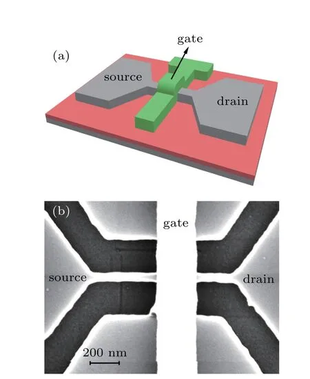
Fig.1. (a)The schematic structure of silicon JNT.(b)The top-view SEM image of silicon JNT after gate formation.
3.Results and discussion
We study the thermally activated electrons transport behaviors through the discrete dopant-induced QDs in the impurity band of the silicon JNT within the temperature range from 6 K to 250 K by the temperature-dependent conductance characteristics of the silicon JNT.The thermally activated electron transport is dominated by phonon-assisted hopping through several dopant-induced QDs.[21]Mott believed that a hopping electron with activation energy Eawould always try to find a lower energy state around the Fermi level by the variable range hopping(VRH)in the absence of longrange Coulomb interaction.[22]At high temperatures,the temperature dependence of conductance G for the nearest neighbor hopping(NNH)exhibits as G ∝exp(−Ea/kBT),where kBis the Boltzmann constant.[23]If the activation energy at low temperatures is reduced as large as the Coulomb interaction energy,the VRH conductance which has been predicted by Efros and Shklovskii(ES)should obey the 1/2 exponent law given bywhere TESis the temperatureindependent ES coefficient.[24]Therefore,with temperature increasing,three kinds of electron hopping transports would be observed in the following consequence: ES-type VRH,Mott-type VRH,and NNH.[21]In our experiment,we find two obvious transition platforms within the critical temperature regimes of A and B for the experimental conductance data,which are extracted from the unified transfer characteristics at the gate voltage positions of the initial transconductance gmpeak in Vg1and valley in Vg2.One crossover temperature TAin the higher temperature regime A corresponds to the transition of thermally-activated-electron transport behaviors from NNH to Mott-type VRH.[25]The other crossover temperature TCin the lower temperature regime B corresponds to the VRH transition for the delocalized electrons from Mott law to the ES law under the influence of Coulomb interaction.[26]The quantitative analysis on the experimental temperaturedependent conductance data has been taken by linear fitting of lnG ∝−Ea/kBT for NNH,lnG ∝−(TM/T)1/4for Mott-type VRH,and lnG ∝−(TES/T)1/2for ES-type VRH.
Figure 2(a)presents the temperature-dependent conductance G(i.e.,G=IDS/VDS)curves obtained from the transfer characteristics at low source–drain bias VDS=1 mV.The clear quantized current steps below the temperature of 75 K indicate the population of the individual sub-bands caused by the quantum confinement effect.[27]Above the temperature of 75 K,the thermal energy is greater than the subbands spacing,resulting in the smearing of the current steps.Figure 2(b)illustrates the corresponding transconductance gm–VGcharacteristics at different temperatures. We define the onset gate voltage Vgtas the initial point of the first gmpeak,where the drain current in the conduction channel is at the onset state.The onset gate voltage Vgtincreases from 6 K to 20 K and decreases from 100 K to 250 K,resulting from the interaction of the induced image charges in the dielectric interface with the impurity and the subband states in the channel.[13]To explore the conductance characteristics under the same filled energy level,we take the onset gate voltage Vgtto unify the transfer characteristics in Fig.2(a)for the alignment of energy levels at different temperatures.In order to clarify the electron hopping transport in the impurity band,figure 2(c)shows the IDS–Vgcurves(upper part)and the corresponding transconductance gm–Vgcurves(lower part)at the temperature of 6 K under the bias VDSvarying from 1 mV to 10 mV.The clear oscillatory current with several splitting peaks(upper part)identifies the coupling of dopant-induced QDs in the impurity band.With the gate voltage increasing,the Fermi energy level of electrons in the quantum confined channel is allowed to enter the conduction subbands,resulting in the current steps.[28,29]
In order to study the temperature-dependent conductance G characteristics in Fig.2(a),we firstly extract the experimental conductance data for different temperatures according to the initial gmpeak at the gate voltage Vg1,in which the effective mobility of hopping electrons is the highest in the impurity band.For comparison,we also provide the temperaturedependent conductance data according to the initial gmvalley at the gate voltage Vg2,in which the electron hopping behavior is suppressed by the Coulomb interaction.Figure 2(d)provides the Arrhenius conductance plots(G vs.1/T)at the gate voltages of Vg1and Vg2within the temperature range from 6 K to 250 K.Interestingly,it is found that the conductance at the temperature of 6 K is much larger than that of 10 K,which may be related with the Coulomb interaction.As the temperature increases,the incomplete ionized donors in the channel are gradually transformed into ionized donors,which result in stronger impurity scattering to reduced the electron mobility.[30]The inset G–T diagrams in Fig.2(d)show two apparent platforms of the conductance for the gate voltages Vg1and Vg2within the temperature regions of around 200 K and around 100 K,as the color marked A and B.The platform of the temperature-dependent conductance for the gate voltage Vg1within the temperature range from 50 K to 100 K is more evident than that of the gate voltage Vg2within the temperature range from 75 K to 125 K,resulting from the stronger quantum confinement at the initial stage of the conduction channel in the silicon JNT.
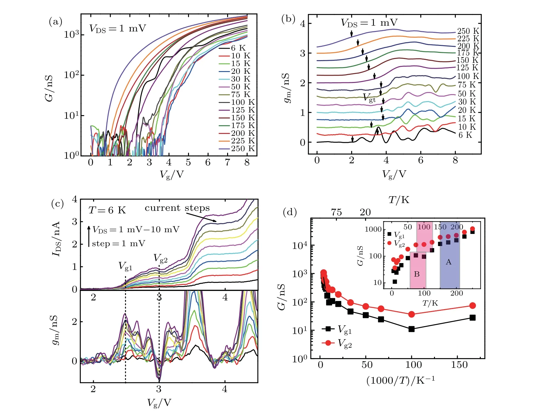
Fig.2.(a)The temperature-dependent conductance G(i.e.,G=IDS/VDS)curves of the device at VDS=1 mV within the temperature range from 6 K to 250 K.(b)The temperature-dependent transconductance gm–VG characteristics at VDS=1 mV,where the transconductance is given by gm=dIDS/dVG.(c)IDS–Vg curves(upper part)and the corresponding transconductance gm–Vg curves(lower part)at the temperature of 6 K under the bias VDS varying from 1 mV to 10 mV.(d)The Arrhenius conductance plots(G vs.1/T)on logarithmic scale at the gate voltages of Vg1 and Vg2 within the temperature range from 6 K to 250 K,The inset shows the corresponding temperature-dependent conductance data(G vs.T),which are extracted from panel(a)after unified by the onset gate voltage Vgt at different temperatures.
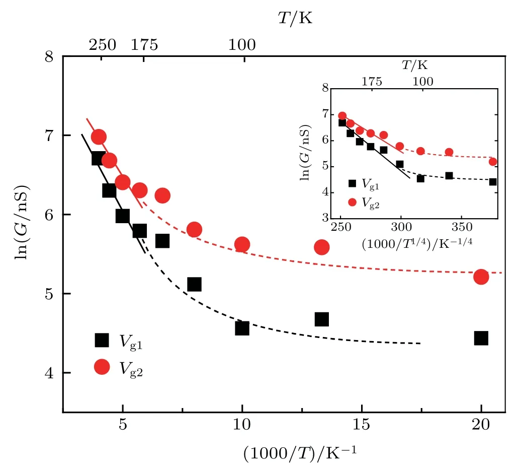
Fig.3.Arrhenius plot of conductance in lnG vs.1/T scales for NNH within the temperature range from 175 K to 250 K.The inset shows Mott-type VRH temperature dependence of the conductance in lnG vs.(1/T)1/4 scales.
In order to precisely determine the transition temperatures TAin temperature region A,we replot the Arrhenius curves of temperature-dependent conductance at high temperature regime as the curves of lnG vs.1/T in Fig.3 for the gate voltages Vg1and Vg2respectively.The inset shows the Motttype VRH temperature dependence of the conductance in lnG vs.(1/T)1/4scales.Here,we are interested in the hopping behaviors of the thermally activated electrons from the ionized dopant atoms.The linearly fitting by lnG ∝−Ea/kBT is shown in Fig.3 for the thermally activated electrons by NNH above the crossover temperature TA,in which the electrons have enough thermal activation energy Eato overcome the potential barriers between the nearest neighbor states.The hopping distance r in NNH is supposed to be equivalent to the mean distance d between neighbored dopant atoms,which can be determined by the doping concentration Ndas
According to the doping concentration Nd=4.16×1017cm−3,the hopping distance between the nearest neighbored dopant atoms is estimated to be 13.4 nm.According to the linearly fitting of the experimental conductance data in Fig.3 within the temperature range from 175 K to 250 K,the activation energies Eafor the hopping electrons are extracted to be 45.2 meV and 33.7 meV respectively for the curves at the gate voltages Vg1and Vg2.[31]According to Mott’s theory,the activation energy Eafor electron hopping is related to the constant density of states(DOS)g0at the Fermi level and the hopping distance
r as[32]

The probability P for hopping is proportional to the conductance G of the device,which depends on the overlap integral of the wavefunctions within the localization radius a and the activation energy Ea,[26]i.e.,

Taking the expression of Ea(Eq.(2))into Eq.(3),one may get the relation between the probability and the hopping distance,P ∝G ∝exp(−2r/a −3/(4πg0r3kBT)).After taking the derivative of the hopping probability dP/dr=0,the optimal electron hopping distanceMis obtained to be[33]
where aMis the localization length in the Mott hopping regime.At the crossover temperature TA,the electron hopping distance of VRH is assumed to be equal to that of NNH,

which is determined by the localization length aMand the density of states g0. In order to determine the localization length aM,we may use the Mott-type VRH conductance expression by substituting Eqs.(2)and(4)into Eq.(3),i.e.,G ∝P ∝exp(−(TM/T)1/4).The temperature factor TMis related to the localization length aMbyAccording to the fitting results from 175 K to 250 K of lnG vs. T −1/4 scales in the inset of Fig.3,the temperature factor TMextracted from the slopes is 38.784K for the gate voltage Vg1and 28.94K and for the gate voltage Vg2.Therefore,the localization length aMcan be obtained from the expression of TMbe about 3.47 nm and 4.66 nm respectively for the gate voltages Vg1and Vg2.The density of states g0at the Fermi energy can be estimated to be 2.2×10¹⁸eV−1·cm−3and 2.96×10¹⁸eV−1·cm−3from Eqs.(2)and(5)by taking the activation energies of 45.2 meV and 33.7 meV respectively for the gate voltages Vg1and Vg2,both of which have the same magnitude as reported in silicon nanowires.[19]As expected from Eq.(6),we obtain the crossover temperatures of TA1=203 K and TA2=202 K respectively for the gate voltages Vg1and Vg2,which are consistent with the experimental observation in the conductance platform A of Fig.2(d).The result shows that the crossover temperature TAfrom NNH to VRH is independent of the gate electric field,which may result from the stronger interactions of the thermally activated electrons.

whose curve is shown in the inset of Fig.4.At the crossover temperature TCfor the VRH transition from Mott-type law to ES-type law,the activation energy Eashould be equivalent to the Coulomb interaction energy ∆,i.e.,
The DOS at the condition of Ea=∆would remain constant as g0in Mott VRH,which is given by
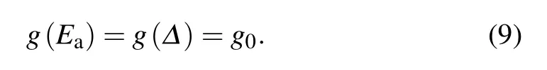
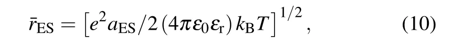
in which the localized length aESin ES hopping regime indicates the average modulation length of long-range Coulomb interaction between the dopant-induced QDs in the conduction channel.In order to determine the localization length aES,we substitute Eqs.(8)and(10)into Eq.(3)to get the ES-type VRH conductance expression

The temperature factor TESis related to the localization length aES by
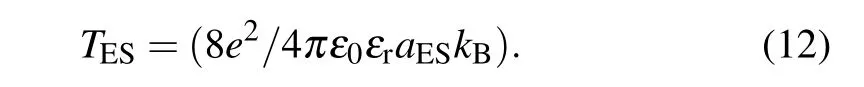
The temperature factor TESextracted from the slopes is 34.8 K for the gate voltage Vg1and 31.4 K for the gate voltage Vg2.Therefore,the localization length aESfor ES-type VRH can be obtained from Eq.(12)to be about 323 nm and 358 nm respectively for the gate voltages Vg1and Vg2.The result indicates that the localization length aESis enhanced with the increase of the gate voltage due to screening of the trapping potentials of the dopant atoms. Considering the expressions from Eq.(7)to Eq.(10),we finally obtain the expression of
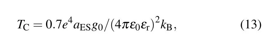
which is determined by the constant DOS g0and the localized length aES.As a result,the crossover temperature of the VRH conductance transition from Mott-type law to ES-type law can be estimated to be TC1=85 K at the gate voltage Vg1and TC2=126 K at the gate voltage Vg2. Both the two crossover temperatures TC1and TC2are consistent with the experimental observation of conductance platform B of Fig.2(d).The crossover temperature TC2of 126 K is much higher than TC1of 85 K,which may result from the stronger Coulomb interaction at the gate voltage Vg2of the gmvalley.
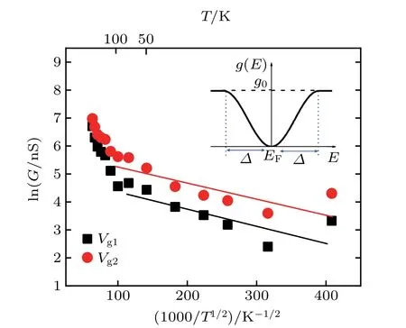
Fig.4.Arrhenius plot of conductance in lnG vs.(1/T)1/2 scales for ES-type VRH,with the inset for the density of states near the Fermi energy level.
4.Conclusion
We present an experimental evidence of hopping transition for the delocalized electrons in silicon JNT by the temperature-dependent conductance characteristics.The theoretical models of Mott-type VRH and ES-type VRH agree well with the experimental data of temperature-dependent conductance,which are extracted from transfer characteristics for different temperatures at the gate voltage positions of the initial transconductance gmpeak in Vg1and the valley in Vg2. The crossover temperature TAfrom NNH to Mott VRH is analytically determined to be 203 K and 202 K constantly for the gate voltages Vg1and Vg2by the conductance transition of the thermally activated electrons.Another crossover temperature TCof VRH behavior from Mott-type law to ES-type law is theoretically determined to be 85 K and 126 K respectively for the gate voltages Vg1and Vg2by considering the Coulomb interactions.As expected,stronger Coulomb interaction at the gate voltage Vg2of the gmvalley leads to the obvious increase of the crossover temperature TCfor the VRH transition behavior.Our finding provides essential evidence for the hopping electron behaviors under the influence of thermal activation and long-range Coulomb interaction.
Acknowledgment
The authors acknowledge Dr. Hao Wang,Dr. Liuhong Ma,and Mr.Xiaoming Li for their supports in device fabrication.
猜你喜欢
疯狂英语·新读写(2022年12期)2022-12-15
Chinese Physics B(2022年1期)2022-01-23
考试与评价·七年级版(2021年5期)2021-08-14
——专访富华国内销售部部长古嘉杰
专用汽车(2020年11期)2020-11-23
——访富华销售总监张航博士
专用汽车(2020年10期)2020-10-26
Chinese Physics B(2019年6期)2019-06-18
专用汽车(2017年3期)2017-03-30
专用汽车(2016年11期)2017-01-11
专用汽车(2016年5期)2016-03-01
专用汽车(2015年4期)2015-07-08

- Chinese Physics B的其它文章
- Compact finite difference schemes for the backward fractional Feynman–Kac equation with fractional substantial derivative*
- Exact solutions of a(2+1)-dimensional extended shallow water wave equation∗
- Lump-type solutions of a generalized Kadomtsev–Petviashvili equation in(3+1)-dimensions∗
- Time evolution of angular momentum coherent state derived by virtue of entangled state representation and a new binomial theorem∗
- Boundary states for entanglement robustness under dephasing and bit flip channels*
- Manipulating transition of a two-component Bose–Einstein condensate with a weak δ-shaped laser∗