
Emerging properties of two-dimensional twisted bilayer materials∗
2019-11-06 00:46YangCheng程阳ChenHuang黄琛HaoHong洪浩ZixunZhao赵子荀andKaihuiLiu刘开辉
Chinese Physics B 2019年10期
Yang Cheng(程阳),Chen Huang(黄琛),Hao Hong(洪浩),Zixun Zhao(赵子荀),and Kaihui Liu(刘开辉)
State Key Laboratory for Mesoscopic Physics,Academy for Advanced Interdisciplinary Studies,School of Physics,Peking University,Beijing 100871,China
Keywords:two-dimensional materials,twist angle,moiré potential,interlayer coupling
1.Introduction
The concept of 2D materials is prevailing accompanied with the discovery of graphene,[1,2]which opens up a new field of material science. 2D materials have many unique physical properties,such as the Dirac cone band structure of monolayer graphene,valley-selective polarized light absorption of transition metal dichalcogenide(TMD),great insulation of hexagonal boron nitride(hBN),and so on.[3–5]Benefitting from the abundance of 2D monolayers,the heterostructures,built by different layer stacking,form a new big family.In sharp contrast to conventional bulk materials,lack of dangling bonds at the surface greatly facilitates the building of heterostructures without further consideration of the lattice mismatch.When one layer is stacked on another forming bilayer,their different lattice vectors can lead to the formation of superlattice,and the electrons in the system will feel an additional potential called moiré periodic potential(Fig.1).Also,surface-exposed electronic states and quantum confinement significantly enhance the interlayer electronic coupling.The moiré periodic potential and enhanced electronic coupling not only tune the intrinsic behavior of the component layers,but also bring many novel physical properties appearing at the interface such as Mott-insulator state,unconventional superconductivity,and moiré excitons.[6–11]Furthermore,these two mechanisms bring us a new approach to engineering the properties of 2D bilayer materials by tuning the interfacial twist angle.With interfacial twist angle tuning,real-space rotation introduces the evolution of moiré pattern and moiré periodic potential,reciprocal-space rotation introduces band alignment change and finally tunes the interlayer coupling.

Fig.1.Moiré patterns and enhanced interlayer coupling in 2D twisted bilayer materials.(a)–(c)Configurations of AA stacking/twisted/AB stacking hexagonal lattice bilayers.(d)Schematics of moiré patterns of 5◦twisted bilayer graphene.(e)Schematics of interlayer couping in 2D twisted bilayer materials.
In this review,we discuss the topic of the 2D twisted bilayer materials,particularly concentrating on how the twist angle determines the physical properties. First,we summarize different methods to fabricate twisted bilayers under different conditions.Then,three typical material systems are discussed:twisted bilayer graphene,graphene/hBN heterostructures,and TMD bilayers.At last,we give our perspectives on the study and applications of 2D twisted bilayer materials.
2.Fabrication of 2D twisted bilayer materials
Fabrication is the first and most fundamental step in material science research.Mainly two challenges exist in the fabrication process of 2D twisted bilayer materials:accurately controlling interfacial twist angle and building clean interface.Generally,if we do not care much about the accuracy of the twist angle,crude methods can satisfy our demands.Common wet transfer or dry transfer method can be used to fabricate twisted bilayer,where polymer is used to pick up one layer from its substrate and stack the layer on another. However,in this way the interface is not clean enough.[12–15]As shown in Fig.2(a),direct chemical vapor deposition(CVD)method can also be used to grow TMD bilayers with different twist angles.[16]In this process,twisted bilayer(non 0◦/60◦twist angle)is a by-product of high-symmetry-stacking heterostructures. The value of the twist angle can be obtained directly according to their relative geometry.Although CVD method can guarantee the clean interface,it gives random twist angle which is uncontrollable.Figure 2(b)illustrates the process used to fabricate magic-angle twisted bilayer graphene.[17]The maximum magic angle is less than 1.1◦,[18]so the fabrication process must be more delicate.The so-called‘tear&stack’technique,first proposed by Kim et al.,[19]is essentially a modified dry transfer method used for twist angle control.Independently,utilizing the strong van der Waals interaction between hBN and graphene,Cao et al.tore half of one piece of monolayer graphene vertically from the substrate,and then rotated the substrate by the largest magic angle with an accuracy of about 0.1◦. At last they stacked the first half on the remaining monolayer to form twisted bilayer and picked it up from the substrate.In this process,hBN was used instead of polymer to obtain a cleaner interface compared to common dry transfer method.[20]
In contrast to the methods mentioned above,twisted graphene/hBN heterostructures can be fabricated in other ways as reported,and such methods allow one to regulate the twist angle after fabrication. As shown in Fig.2(c),utilizing the weak friction between hBN and graphene,atomic force microscope(AFM)tip can be used to control the twist angle of the heterostructures mechanically.[21,22]In this process,graphene is placed on top of hBN with a large twist angle to avoid disturbance.Then the graphene layer is etched into a Hall bar with oxygen plasma for electronic measurements,and a preshaped hBN flake is transferred onto the graphene.Thus AFM tip can rotate the preshaped flake to control the twist angles after fabrication.In addition,utilizing the potential difference among heterostructures with different twist angles,thermal annealing is also adopted as shown in Fig.2(d).[21,23]

Fig.2.Fabrication methods.(a)Top:illustration of CVD growth of vertical WS2/MoS2 bilayers.Bottom:schematic illustration,optical image,and scanning electron microscopy image of vertical WS2/MoS2 bilayers.Reprinted with permission from Ref.[16].Copyright 2016,Nature Publishing Group.(b)Schematic illustration of‘tear&stack’technique,which is essentially a modified dry transfer method to fabricate clean interface with accurate twist angle.Reprinted with permission from Ref.[17].Copyright 2016,American Physical Society.(c)Schematic illustration and AFM images of the twist-angle-tunable graphene/hBN heterostructures.Reprinted with permission from Ref.[22].Copyright 2018,American Association for the Advancement of Science.(d)Top:AFM images of graphene/hBN heterostructures before(left)and after(right)annealing.Bottom:AFM images of graphene/hBN heterostructures.They are obtained initially(left),after AFM tip control(middle),and after long-time annealing(right),respectively.Reprinted with permission from Ref.[23].Copyright 2016,Nature Publishing Group.Reprinted with permission from Ref.[21].Copyright 2016,American Physical Society.
3.Physical properties of 2D twisted bilayer materials
3.1.Twisted bilayer graphene
Monolayer graphene is a 2D Dirac semimetal with many unique properties,such as massless Dirac fermion,high carrier mobility,and wide-spectrum light absorption compared to the conventional materials.[24]As for common intrinsic Bernal stacked bilayer graphene(AB stacking),the bandgap remains zero while the fermion becomes massive.[3]However,when taking the twist angle into consideration,new physical phenomena have been found and investigated in twisted bilayer graphene.
3.1.1.New van Hove singularities
As shown in Fig.3(a),it has been reported that within a broad range(from 1◦to 10◦)of twist angles,two robust new van Hove singularities arise owing to the hybridization of the energy bands of these two layers.[25–27]The energy level of the two van Hove singularities can be obtained by scanning tunneling spectroscopy(STS),while the experimental results of the energy separation between them(∆E)accord with the theoretical prediction(based on the continuum model)[28,29]
where vFis the Fermi velocity of monolayer graphene,Γ K is the wave vector of the Dirac point in reciprocal space of graphene,θ is the twist angle,and tθis the amplitude of the main Fourier component of the interlayer potential. The effect of such band structure can also be observed in optical spectroscopy,like absorption spectra,angle-resolved Raman imaging,and angle-tunable photoluminescence with resonant 2-photon excitation.[30–33]The van Hove singularity boosts the density of states of materials,and thus provides a strong light–matter interaction in twisted bilayer graphene.It has been reported that twisted bilayer graphene can enhance the signal in ultrafast photodetection utilizing this property.[34]

Fig.3. Physical properties of twisted bilayer graphene. (a)Schematic illustration and STS results of the new van Hove singularities of twisted bilayer graphene.The interlayer interaction leads to the formation of van Hove singularities,and they correspond to the two peaks in STS measurements.The relation between the singularity energy separation and the twist angle is also shown.Reprinted with permission from Ref.[27]. Copyright 2012,American Physical Society. (b)Left,calculated band structure and density of states of twisted bilayer graphene with twist angle θ=1.05◦. Top right,two-probe longitudinal conductance results of twisted bilayer graphene with twist angle θ=1.16◦.Insulating states have been marked by background color.Bottom right,four-probe longitudinal resistance results of two twisted bilayer graphene samples with twist angles θ=1.05◦and θ=1.16◦. Reprinted with permission from Ref.[7]. Copyright 2018,Nature Publishing Group.(c)Left:illustration of quasicrystal twisted bilayer graphene.Top right:ARPES results of quasicrystal twisted bilayer graphene.Bottom right:illustration of Umklapp scattering process,which is responsible for the extra scattering points in the ARPES.Reprinted with permission from Ref.[51].Copyright 2018,American Association for the Advancement of Science.
3.1.2.Magic angle and flat band
In 2010,Morell et al.predicted the occurrence of flat bands(simultaneously,zero Fermi velocity at Dirac point)in twisted bilayer graphene using tight-binding calculations,which probably means the existence of strong electron–electron interaction.[35]In 2011,Bistritzer et al.solved the continuum Dirac model for twisted bilayer graphene and also found a flat band for a series of the so-called magic angles,[18]which was partly(only for the largest twist angle)convinced in 2015 using STS by Yin et al.[36]Later,Cao et al.successfully realized the material system and made various electrical measurements on it.[6,7]At first,they found that the conductance of twisted bilayer graphene becomes zero with the moiré band half-filled and attributed this to the formation of a Mott insulator,which can be explained in rough as the consequence of the split of the moiré band caused by the repulsion of the two electrons in the same orbital state with different spins(Hubbard model).[37,38]Then they made more careful measurements(four-probe resistance Rxx)and observed an unconventional superconducting state whose doping density is slightly away from the lower Mott-insulator state(Fermi level EF<0)with the critical temperature below 1.7 K.The band structure,the two-probe conductance results,and the four-probe resistance results are shown in Fig.3(c). As they have pointed out,such tunable system offers a brand-new platform to study unconventional superconductivity,which has attracted many researchers to do related work on it(e.g.,a superconducting state is also observed at a twist angle slightly larger than 1.1◦under higher pressure).[39–48]
3.1.3.Graphene quasicrystal
The twist angles mentioned above are mostly small angles. As for large twist angles,the interaction between two layers is usually weak.[49,50]Ahn et al.fabricated twisted bilayer graphene with a twist angle of exactly 30◦,which forms a graphene quasicrystal with dodecagonal quasicrystalline order and anomalous interlayer interaction is found by angleresolved photoemission spectra of the system.[51]Extra scattering points owing to Umklapp scattering process of the two layers are shown in Fig.3(b). Yao et al.have also reported successful growth of such graphene quasicrystal and investigated the emergence of mirrored Dirac cones.[52]They identified that these mirrored Dirac cones are a consequence of the interlayer interaction showing its importance in the incommensurate structure which had been overlooked before.
3.1.4.Other emerging properties
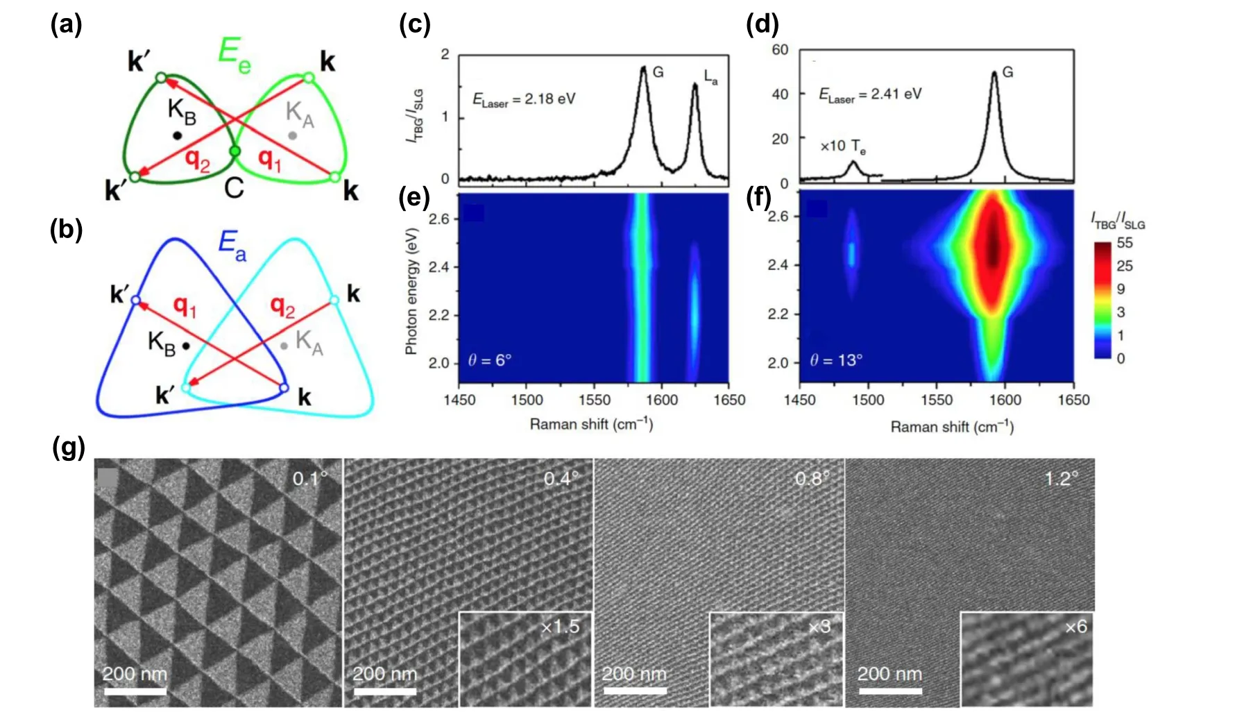
Fig.4.Electron–phonon coupling and atomic reconstruction in 2D twisted bilayer materials.(a)and(b)Schematics of interlayer electron–phonon process where a phonon with momentum connects the states k and of different layer(a)and intralayer electron–phonon process where both states k and are from the same layer.(c)and(d)Raman spectra of twisted bilayer graphene with θ=6◦and 13◦measured with the 2.18 eV and 2.41 eV laser lines,respectively.The vertical coordinate corresponds to the ratio of the peak intensities of the Raman spectra in twisted bilayer graphene and monolayer graphene.(c)The peak around 1620 cm−1 is called La and stems from intralayer electron–phonon scattering process and(d)the peak at 1480 cm−1 is called Te and stems from the interlayer electron–phonon scattering process.(e)and(f)Excitation Raman maps of twisted bilayer graphene with θ=6◦(e)and 13◦(f)measured under different laser energy excitations.Reprinted with permission from Ref.[54].Copyright 2019,Nature Publishing Group.(g)TEM dark-field images of twisted bilayer graphene with different twist angles obtained by selecting diffraction peak(g=100).Different contrast stands for different stacking order(AB/BA).Reprinted with permission from Ref.[45].Copyright 2019,Nature Publishing Group.
In addition to the band structure of electrons,electron–phonon coupling is also a fundamental interaction that affects a broad range of phenomena in condensed matter physics,such as electron mobility,and is responsible for conventional superconductivity.[53]In multilayer structures,the interaction can involve intralayer electron–phonon interaction or interlayer electron–phonon interaction(Figs.4(a)and 4(b)).Eliel et al.reported the ability of Raman spectroscopy to probe and distinguish interlayer and intralayer interactions in graphenebased heterostructures.[54]As shown in Figs.4(c)and 4(d),they measured Raman spectra in two samples of twisted bilayer graphene with twist angles θ=6◦and 13◦recorded with the 2.18 eV and 2.41 eV laser lines,respectively.The frequencies of these phonons depend on the twisting angle θ.[55–63]In addition,they made multiple-excitation Raman measurements using multiple laser lines and found that the results show different dependence on the incident photon energy(Figs.4(e)and 4(f)).Bilayer graphene and graphene/hBN samples with different twist angles also show similar results.
The theoretical results of twisted bilayer graphene mentioned above are all based on a common assumption that the lattice structure of either layer does not change significantly despite the interlayer interaction.However,Yoo et al.reported that this is not the case.[45]In Fig.4(g),the transmission electron microscope(TEM)dark-field images are obtained by selecting the diffraction peak from a series of twisted bilayer graphene samples with multiple twist angles. In these images,different contrasts stand for totally different stacking order(AB/BA)domains,and for the twisted bilayer graphene sample with 0.1◦twist angle,the sharp boundaries indicate the existence of atomic reconstruction,in contrast to the relatively continuous distribution of stacking order if not reconstructed. As the twist angle increases,the boundaries become blurry,which represents the weakening of interlayer interaction.Based on this discovery,they recalculated the band structure of twisted bilayer graphene with small twist angles and found that a simple moiré band description breaks down and the secondary Dirac bands appear when the twist angle θ<θc(θc≈1◦).
3.2.Graphene/hBN heterostructures
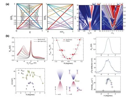
Fig.5.Physical properties of graphene/hBN heterostructures.(a)Left,normalized Hofstadter butterfly spectrum for square lattice in a magnetic field.Middle,density-field diagrams of such system.Colored lines stand for constant chemical potential for both two above.Right,transport measurement results of graphene/hBN heterostructures.The slope of each line has been marked in the figure.Reprinted with permission from Ref.[68].Copyright 2013,Nature Publishing Group.(b)Top left,four-probe resistance as a function of gate voltage(Vg)results.A satellite peak locates away from charge neutrality point and indicates an extra energy gap.Bottom left,energy gap as a function of twist angle.Top middle,satellite peak position as a function of twist angle.Bottom middle,illustration of energy gap.Right,four-probe resistance(R4P),tip deflection(reflection of friction force),and full width at half maximum of the 2D peak(FWHM2D)in Raman spectroscopy as a function of twist angle at a carrier density of −1.9×1012 cm−2. Reprinted with permission from Ref.[22].Copyright 2018,Nature Publishing Group.
The study of graphene/hBN heterostructures became popular after Dean et al.pointed out that hBN can be an appealing substrate for graphene,fairly avoiding various factors which will decrease the quality of graphene in contrast to the standard SiO2substrate.[64]The experimental results indicate that the coupling between graphene and hBN is generally weak for the band structure of graphene. In 2013,several papers were published discussing the transport properties of graphene/hBN heterostructures, and they particularly concentrated on the so-called Hofstadter butterfly[65]induced by the moiré periodic potential and an external magnetic field,as shown in Fig.5(a).[66–68]However,despite the crucial role which moiré pattern plays in the realization of the Hofstadter butterfly,the twist angle,an important factor to tune the moiré periodic potential was not introduced then. This can be attributed to the reasons below. Firstly,the realization of the Hofstadter butterfly demands a large periodicity,and thus the twist angle cannot be larger than 2◦for graphene/hBN heterostructures.Most importantly,the method to precisely regulate the twist angle after fabrication had not been proposed then.In 2016,AFM tip was introduced and thus the properties of the heterostructures with respect to the twist angle were studied,as shown in Fig.5(b)(the fabrication method has been illustrated in Fig.2(d)).[22]In their experiments,large twist angles exhibit weak coupling between layers accounting for the so-called superlubricity which has also been investigated in other 2D systems,[69–72]while for small twist angles,the interlayer interaction opens a small bandgap at the doping density where locates the satellite peak of the longitudinal resistance.The satellite peak has been reported before as the consequence of the moiré potential,and thus the bandgap significantly depends on the twist angle.In addition,the Raman intensity of the 2D peak,and mechanical properties measured by the AFM tip exhibit similar dependence on the twist angle as well.Despite all this,further investigations are still demanded to explain these experimental results.
3.3.TMD bilayers
After the discovery of graphene,the appearance of TMD materials markedly broadens the 2D materials with diverse physical properties.[73–76]Most TMD materials are semiconductors whose bandgaps cover the range from near-infrared to visible region with strong light–matter interaction,the degenerate exciton transitions at the K andvalleys in the momentum space with broken inversion symmetry in TMD materials offer a new platform for exploring spin and valley physics,TMD materials have several phases which can be tuned by electric field,pressure,or light.[77–79]
3.3.1.Electronic and mechanical coupling in twisted MoS2 bilayer
Liu et al.investigated photoluminescence and Raman spectra of 44 MoS2bilayers with different twist angles(Figs.6(a)and 6(b)).[80]They reported that the A exciton recombination photoluminescence peak position(peak I in Fig.6(c))remains the same for all bilayers with different twist angles,but photoluminescence intensity decreases significantly compared with the monolayer one.For the bilayer case,a lower-energy peak appears(peak II in Fig.6(c)),which corresponds to an indirect bandgap recombination resulting from the interlayer electronic coupling.They found that the indirect bandgap varies with twist angle.AA/AB stacking bilayers have smaller bandgap than that of twist ones,indicating stronger interlayer electronic coupling. In addition,Raman spectra of MoS2monolayer and bilayers with different twist angles have been investigated to identify the effective interlayer mechanical coupling,that is,larger separation between two Raman peaks(ωA−ωE)means stronger coupling strength(Fig.6(d)).This twist-angle-dependent coupling is attributed to the varied interlayer distance in van der Waals coupled 2D atomic-layered materials due to steric effect:the increase of the interlayer distance will weaken the coupling strength.From their experimental results,AA or AB stacking MoS2bilayer has stronger electronic and mechanical coupling than the twist angles ones. This conclusion is also suitable for other TMD bilayers.[81–83]

Fig.6.Electronic and mechanical coupling in twisted MoS2 bilayer.(a)Schematics of MoS2 bilayers with different stacking configurations.Green spheres are Mo atoms;yellow sphere are S atoms.(a)Optical images of a MoS2 monolayer and twisted bilayers with different twist angles.(c)Photoluminescence and(d)Raman spectra of MoS2 monolayer and bilayers with different twist angles.Reprinted with permission from Ref.[80].Copyright 2014,Nature Publishing Group.
3.3.2.Stacking-independent ultrafast charge transfer in twisted TMD heterostructures
TMD heterostructures are of particular interests because many of them form type II heterojunctions,which facilitate the efficient separation of photoexcited electrons and holes and therefore exhibit great potential in the applications of photodetectors,photovoltaics,and sensors. This separation in MoS2/WS2bilayers could take place within 50 fs upon photoexcitation due to strong interlayer coupling.[84–86]As the interlayer coupling in 2D heterostructure materials varies with interlayer twist angles,Ji et al.have investigated how the interlayer charge transfer in MoS2/WS2bilayers evolves with different stacking configurations(Fig.7(a)).[87]In Fig.7(b),two obvious peaks in MoS2/WS2bilayers photoluminescence spectra correspond to direct A-exciton transitions from MoS2(peak I)and WS2(peak II),respectively. Intensity of Peak I in the heterostructures is 1/5 of that in MoS2monolayer indicating strong interlayer electronic coupling and efficient electron–hole separation.The transient absorption spectra of MoS2and MoS2/WS2bilayers with different twist angles are shown in Fig.7(c).Interestingly,they observed that the rise time of MoS2/WS2bilayers with different twist angles only varies slightly,suggesting that the charge transfer time is robust and stacking independent. This robust ultrafast charge transfer is contrary to time-dependent density functional theory simulations and naive thinking that stronger interlayer coupling induces faster charge transfer.[88]In Fig.7(d),scanning transmission electron microscopy(STEM)image of an AA stacking MoS2/WS2bilayer indicates that in addition to the energy-favourable AA1stacking,there exists high-energy stacking of AA3due to interlayer stretching and shifting.The existence of multiple parallel charge transfer channels results in the robust ultrafast stacking-independent charge transfer,as the measured charge transfer time is mainly determined by the fastest channel(Fig.7(e)).Same results have also be reported by Zhu et al.[89]
3.3.3.Moiré phonons in twisted MoS2 bilayer
In TMD bilayers,there exists a moiré periodic potential as well,so electron–phonon coupling and phonon–phonon interactions can be affected. Lin et al.discovered that the moiré periodic potential in twisted MoS2bilayer can modify the properties of phonons in its MoS2monolayer constituent to generate Raman modes related to moiré phonons.[90]They measured the Raman spectra in the region of 50–425 cm−1of the twisted MoS2bilayers with twist angles ranging from 9◦to 49◦under the excitation energy E=2.54 eV.Apart from those modes observed in all twisted MoS2bilayers independent of θ like longitudinal acoustic(LA)and transverse acoustic(TA)modes,they observed seven series of θ-dependent Raman modes(Figs.8(a)and 8(b)). It can be attributed to that there are seven moiré phonons in the twisted MoS2bilayer. These phonons originate from the phonons in monolayer constituents with the basic vectors of moiré reciprocal lattices folded onto the zone center due to the modulation of the periodic moiré potentials(Figs.8(c)and 8(d)).Due to the weak interlayer coupling in twisted MoS2bilayer,the phonon dispersions of the monolayer constituents can be probed by the θ-dependent frequency of moiré phonons.In addition,all these moiré phonons exhibit a mirror behavior with regard to θ=30◦.
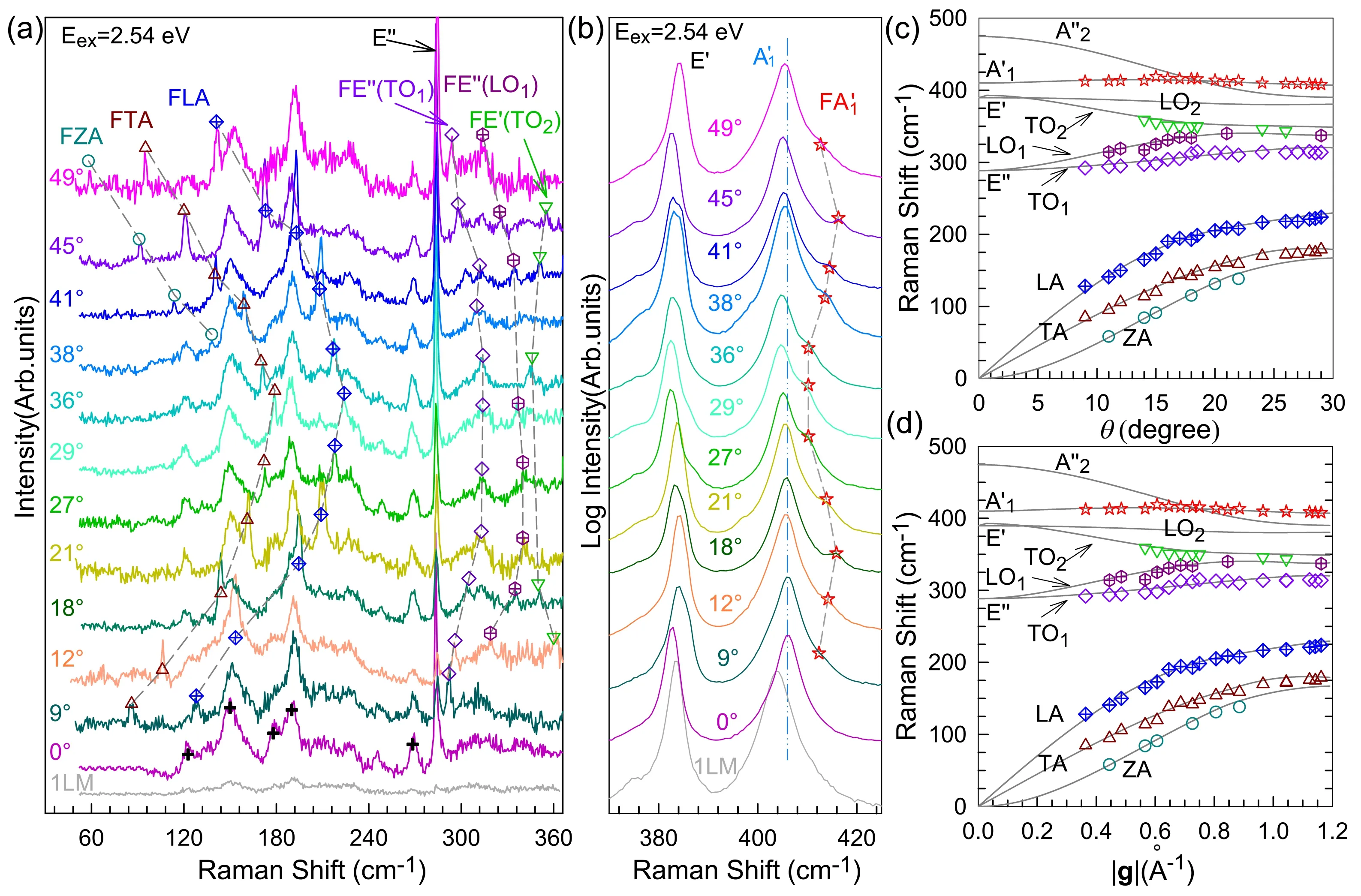
Fig.8.Moiré phonons in twisted MoS2 bilayer.(a)and(b)Raman spectra of twisted MoS2 bilayer in the regions of(a)50–365 cm−1 and(b)370–425 cm−1. The Raman modes in different phonon branches are represented by different shapes and color symbols.The Raman spectra of monolayer MoS2 and 3R-bilayer MoS2(θ=0◦)are plotted for comparison.(c)and(d)The comparison of calculated and experimental frequencies of moiré phonons dependent on θ(c)and|g|(d),|g|is the magnitude of the basic vector of the moiré reciprocal lattices.Reprinted with permission from Ref.[90].Copyright 2018,American Chemical Society.
3.3.4.Moiré excitons in twisted TMD heterostructures
Exciton is the particle-like entity that formed by an electron bound to a hole.[91]Moiré excitons are excitons whose energy levels are quantized arising from the lateral confinement imposed by the deep moiré potential.[8,11]Jin et al.reported experimental observation of moiré excitons in WSe2/WS2bilayers.[8]The optical photograph and schematic diagram are shown in Figs.9(a)and 9(b),and the WSe2/WS2bilayers are encapsulated in thin hBN layers for protection.The twist angle is identified by the STEM image in Fig.9(c),which shows a uniform triangular lattice pattern with a well-defined periodicity of about 8 nm.In the WSe2/WS2bilayers with near-zero twist angle,WSe2A exciton state splits to three prominent peaks(labelled as I,II,and III,respectively)corresponding to distinct moiré exciton states,while only a single resonance peak appears in large twist angle heterostructures(Fig.9(d)).They found that the gate-dependent behaviors of these moiré exciton states are distinct from that of the A exciton in WSe2monolayers and WSe2/WS2bilayers with large twist angles(Fig.9(e)).These phenomena can be fully described by a theoretical model in which the moiré periodic potential(250 meV)is much stronger than the exciton kinetic energy(8 meV)and generates multiple flat exciton minibands.Other three groups also reported the observation of moiré excitons in TMD heterostructures at the same time.[9–11]These observations provide a promising platform for exploring several theoretical proposals related to quantum photonics,such as topological excitons,giant spin–orbit coupling,and entangled photon sources.
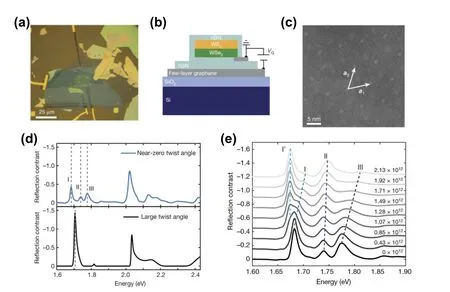
Fig.9.Moiré excitons in twisted TMD heterostructures.(a)and(b)Optical microscopy image(a)and side-view illustration(b)of a representative heterostructure with a near-zero twist angle.(c)A zoomed-in image of atomicresolution STEM of near-zero twist angle WSe2/WS2 bilayers showing the moiré superlattice.The two superlattice vectors are labelled.(d)Reflection contrast spectrum of near-zero twist angle WSe2/WS2 bilayers(top)compared to a large twist angle one(bottom).(e)Reflection contrast spectra in the range between 1.6 eV and 1.8 eV of the WSe2.A exciton upon electron doping.The electron concentration is noted for each spectrum in units of cm−2.Reprinted with permission from Ref.[8].Copyright 2019,Nature Publishing Group.
4.Conclusion and perspectives
As introduced above,engineering physical properties of 2D bilayers by interfacial twist angle has become a hot topic in recent years.This is mainly achieved by two mechanisms,tuning interlayer coupling and moiré periodic potential by tuning the twist angle. Although various novel physics have been found in the 2D heterostructure family,many of them such as the unconventional superconductivity and stackingindependent ultrafast interfacial charge transfer still demand deeper understanding.Also,developing a universal approach to continuously tuning the twist angle and thereby modulating their physical properties is required.At last,massive production of clean interface with accurate twist angle and large-area single crystal is the main challenge for the real applications based on 2D heterostructure family,which should be on the schedule to be explored.

- Chinese Physics B的其它文章
- Compact finite difference schemes for the backward fractional Feynman–Kac equation with fractional substantial derivative*
- Exact solutions of a(2+1)-dimensional extended shallow water wave equation∗
- Lump-type solutions of a generalized Kadomtsev–Petviashvili equation in(3+1)-dimensions∗
- Time evolution of angular momentum coherent state derived by virtue of entangled state representation and a new binomial theorem∗
- Boundary states for entanglement robustness under dephasing and bit flip channels*
- Manipulating transition of a two-component Bose–Einstein condensate with a weak δ-shaped laser∗