
Low insertion loss silicon-based spatial light modulator with high reflective materials outside Fabry–Perot cavity∗
2019-11-06 00:44LiFeiTian田立飞YingXinKuang匡迎新ZhongChaoFan樊中朝andZhiYongLi李智勇
Chinese Physics B 2019年10期
Li-Fei Tian(田立飞),Ying-Xin Kuang(匡迎新),Zhong-Chao Fan(樊中朝),and Zhi-Yong Li(李智勇)
1State Key Laboratory on Integrated Optoelectronics,Institute of Semiconductors,Chinese Academy of Sciences,Beijing 100083,China
2Engineering Research Center for Semiconductor Integrated Technology,Institute of Semiconductors,Chinese Academy of Sciences,Beijing 100083,China
Keywords:spatial light modulator,high reflective materials,silicon-based,Fabry–Perot cavity
1.Introduction
Spatial light modulators play a significant role in application fields of space optical communication,optical calculation,biochemical sensing and digital holography imaging.[1–7]With the rapid development of information era,spatial light modulators are expected to promote the performance improvement of products including unmanned aerial vehicles,micro-satellites,and optical broadband networks.[8–13]Spatial light modulators can modulate the light intensity,phase,and polarization.[14–18]Spatial light modulators can be divided into reflective and transmissive modes according to the different ways of reading out light. Compared with the transmission type,the reflection-type spatial light modulator is a new device with high resolution,contrast,pixel opening rate,and energy utilization efficiency.[19–23]The optical structure of silicon-based spatial light modulator contains a Fabry–Perot(FP)cavity,Mach–Zehnder interferometer,Bragg optical grating,and micro-ring resonant cavity.[24–31]The silicon-based spatial light modulators can be fabricated through a mature microelectronic fabrication technology called complementary metal–oxide–semiconductor process which has low cost,high integration,and high processing precision.However,the extinction ratio of the present spatial light modulator is low and the insertion loss is high for practical applications due to materials problems.[32–37]
Here in this work,we propose a reflection-type siliconbased spatial light modulator with Fabry–Perot cavity structure.We adopt the dielectric thin film to replace the traditional metal film in order to reduce the insertion loss.[33]At the same time,we use the polycrystalline silicon(poly-Si)film as an inside-cavity layer to obtain longer service life than the previous polymer material.The reflectivity values of the outsidecavity materials with different film layer numbers are simulated.The reflectivity,refractivity,surface,and cross-section morphologies,and surface roughness values of the outsidecavity materials are measured.The effect of driving voltage on reflectivity of the spatial light modulator is investigated to gain the extinction ratio and insertion loss.
2.Device design and simulation
Figure 1(a) demonstrates the schematic diagram of designed cross-sectional spatial light modulator unit with FP cavity. The materials outside the cavity, i.e., 6-pair Ta2O5/SiO2thin films constitute the reflecting mirror. The material inside the cavity,i.e.,poly-Si film,is used as an isolation layer.The heating electrode on the surface of isolation layer is of Au/Ti.The substrate is of monocrystalline silicon.Figure 1(b)displays the heating electrode on the surface of isolation layer.The device contains a 50×5 array with single pixel size of 0.2 mm×2 mm.
The reflectivity spectra of the outside-cavity materials with different film layer numbers are simulated according to transfer matrix method(TMM)[38]in order to obtain the optimal values.The simulation architecture includes the silicon substrate,the Ta2O5/SiO2multilayer films,and the air. The reflectivity of outside-cavity material R can be expressed as follows:

where η0is the effective refractivity of the incident medium,i.e., air; B and C are characteristic matrix elements of Ta2O5/SiO2multilayer film,which can be calculated from the following formula:

where k is the layer number of Ta2O5/SiO2multilayer films,is the phase thickness of the j-layer film,ηjis the effective refractivity of the j-layer film,ηk+1is the effective refractivity of the last layer film,i.e.,substrate,and i is the imaginary factor.

Fig.1.Schematic diagram of designed spatial light modulator unit with FP cavity:(a)schematic diagram of cross section and(b)schematic diagram of heating electrode on surface of isolation layer.
The value of δjcan be calculated from the following equation on condition that the incident angle is zero:

where n j is the refractivity of the j-layer film,djthe vertical thickness of the j-layer film,and λ the wavelength of the incident light.The effective refractivity of the film is equal to the refractivity as the incident angle is zero.
Figure 2(a)exhibits the simulation curves of the reflectivity of the outside-cavity material R versus the wavelength of the incident light for the film layer odd number k from 1 to 15.The SiO2and Ta2O5films are arranged alternatively.The first layer is SiO2film with low refractivity,the second layer is Ta2O5film with high refractivity,and so on.The reflectivity of the outside-cavity material at 1550 nm can exceed 91.4%as the odd number of outside-cavity material is not less than 11.
Figure 2(b)shows the simulation curves of the reflectivity of outside-cavity material R versus the wavelength of incident light with the film layer even number k from 2 to 14. The reflectivity of outside-cavity material at 1550 nm can exceed 92.4%as the even number of the outside-cavity materials is not less than 8.
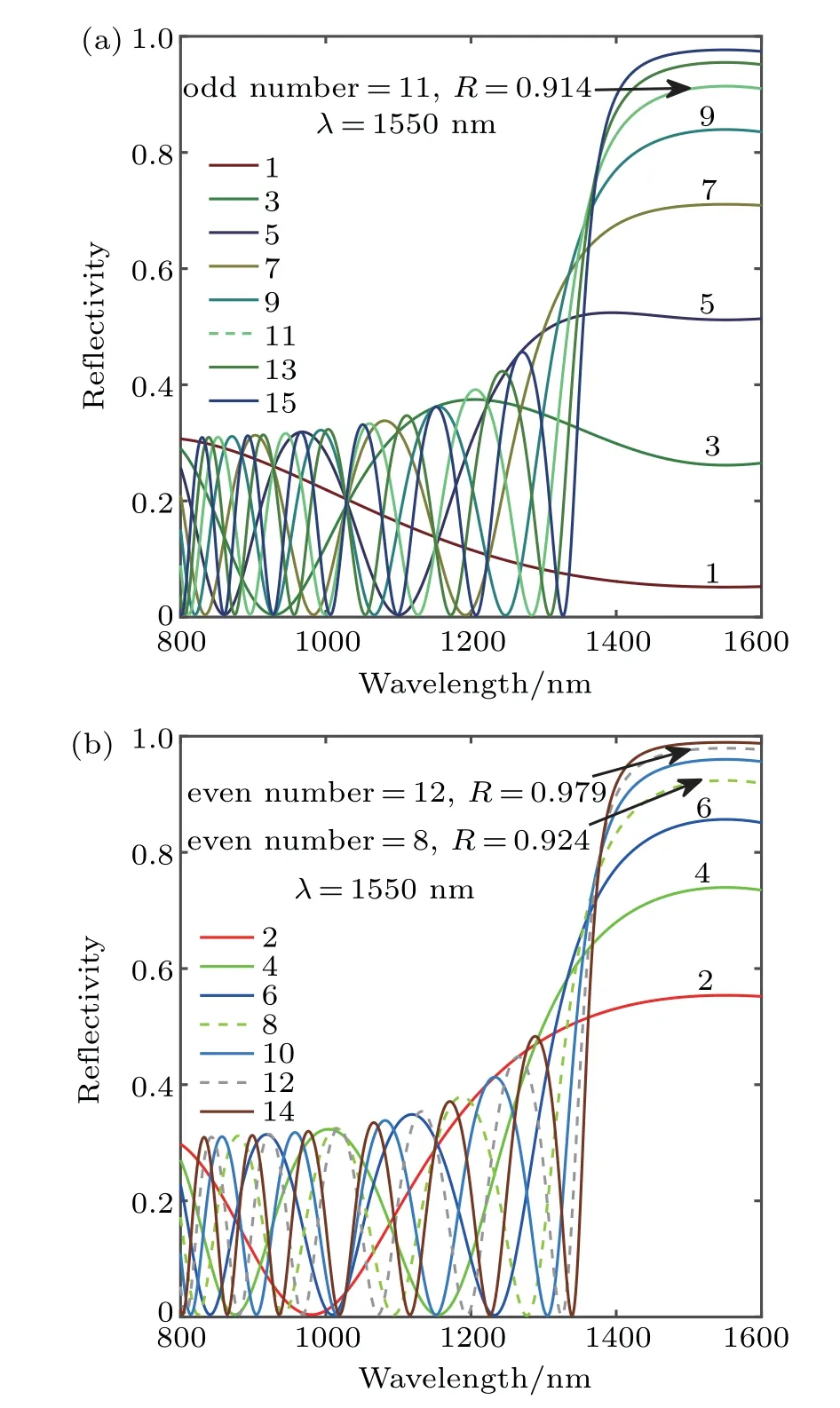
Fig.2. Simulation curves of reflectivity of outside-cavity material R versus wavelength of incident light for film layer(a)odd number from 1 to 15 and(b)even number from 2 to 14.
The even-number film layers are apparently better to realize high reflectivity than the adjacent odd-number film layers.The outside-cavity materials with even number of 12 are chosen to realize both low stress and high reflectivity(97.9%)at 1550 nm.
3.Experiment
The thin films of lower 6-pair Ta2O5/SiO2,poly-Si,and upper 6-pair Ta2O5/SiO2were deposited on the a-plane silicon substrate orderly.The SiO2and Ta2O5thin films with thickness of 260 nm and 190 nm were deposited by ion beam sputtering process.The poly-Si film with a thickness of 100 nm was deposited by chemical vapor deposition.The electrode of Ti and Au films with thickness of 50 nm and 350 nm were deposited by electron beam evaporation.The pattern structures of upper 6-pair Ta2O5/SiO2and electrode were fabricated by ultraviolet lithography and inductively coupled plasma etch technology,successively.
The refractivity values of the thin films were measured using ellipsometer(J A Woollam,M-2000DI).The surface and cross-section morphologies were analyzed by scanning electron microscopy(SEM,FEI,NanoSEM650).The surface roughness values of the thin films were gained by atomic force microscopy(AFM,Bruker,DimensionEdge).The reflectivity values of the outside-cavity materials with wavelength ranging from 800 nm to 1600 nm were analyzed by spectrophotometer(PerkinElmer,Lambda 1050). The incident light of the spatial light modulator was generated from a tunable laser(Yokogawa,AQ2200-136)and a fiber collimator.The reflectivity values of the spatial light modulator with wavelength ranging from 1550 nm to 1600 nm were obtained by optical spectrum analyzer(Yokogawa,AQ6370 C).The voltages exerted on spatial light modulator were introduced from a direct current power supply(Gwinstek,GPD3303 S).
4.Results and discussion
Figure 3(a)displays the variations of measured refractivity with wavelength of SiO2and Ta2O5thin film. With the increase of wavelength from 800 nm to 1600 nm,the refractivity value of SiO2and Ta2O5thin film both reduce gradually and slightly,neither of their decrements is more than 0.22.The refractivity values of SiO2and Ta2O5thin film at 1550 nm are 1.4847 and 2.0723,respectively.
Figure 3(b)shows the simulated and measured reflectivity spectrum of the 6-pair Ta2O5/SiO2thin film.The simulated and measured reflectivity at 1550 nm are 97.9%and 99.9%,respectively.They are highly consistent with each other and the degree of disparity is solely 2%.The measured reflectivity at 1550 nm is slightly higher than the simulated reflectivity.
集体备课是教师个人空间建设专业性的体现,它能够将教师与日常生活进行联系,对传统的备课模式进行创新,使备课的主体呈现多元化。不仅仅局限于本校教师,将备课的范围进行了扩大,集合了更多的力量,使备课质量得到显著提高。在进行功能的设计时,可以采用再现编辑模式,使教师都能够参与教案的修改与制定。教师在进行教学中要结合本班情况对教案进行有针对性的设计。这些操作都在网络上进行,并将最终的教研结果保留在平台上,最终制成数据库,从而提高教学资源的利用率,促进教学资源更好地为实际教学系统服务。
The surface and cross-section morphology,and surface roughness of the outside-cavity materials are measured to ascertain why the measured reflectivity is higher than simulated reflectivity.
Figure 4(a)shows the cross-section SEM image of the 6-pair Ta2O5/SiO2thin films.The inset shows the surface SEM image of the thin films.The surface particle size of the 6-pair Ta2O5/SiO2thin films is fine(less than 2 nm)and uniform.It indicates that the 6-pair Ta2O5/SiO2thin films are extremely compact,which can reduce the bulk scattering loss of light and raise the reflectivity of films.[39]

Fig.3. (a)Measured refractivity versus wavelength of SiO2 and Ta2O5 thin films,(b)simulated and measured reflectivity spectrums of 6-pair Ta2O5/SiO2 thin film.
Figure 4(b)demonstrates the two-dimensional and threedimensional(inset)AFM image of the 6-pair Ta2O5/SiO2thin films. The surface root-mean-square roughness(RMS)is small,only 0.53 nm.The surface roughness is not considered in the simulation method.The reflectivity including the influence of surface roughness is defined by the equation in the normal incident case[40,41]

where Rris the reflectivity of real film,Rpthe reflectivity of film with perfectly smooth surface,σ the RMS of film,and λ the wavelength of incident light.The smaller the RMS of film,the lower the total integrated scattering of light(4πσ/λ)2is and the higher the reflectivity of real film Rr.The surface of the 6-pair Ta2O5/SiO2thin films is comparatively smooth,which can lessen the surface scattering loss of light and enhance the reflectivity of films.

Fig.4.Morphologies and surface roughness of 6-pair Ta2O5/SiO2 thin films:(a)cross-section and surface(inset)SEM image,and(b)twodimensional and three-dimensional(inset)AFM image.
The reflectivity values of spatial light modulator at different voltages are investigated in order to calculate the extinction ratio and insertion loss.The extinction ratio ER is defined by the equation:

where R0is the reflectivity without voltage,and R1is the reflectivity with voltage.
The insertion loss IL is expressed by the formula:

Figure 5(a)shows the reflectivity spectra of the spatial light modulator with the logarithmic vertical axis in a voltage range from 0 V to 6 V.The test point is in the center of a single pixel. The reflectivity values of device within the range from 1550 nm to 1600 nm are nearly constant as the voltage increases from 0 V to 6 V.
Figure 5(b)displays the reflectivity spectra of the spatial light modulator in a voltage range from 8 V to 11 V.The reflectivity values of device within the range from 1550 nm to 1600 nm present a degrading trend as the voltage rises from 8 V to 11 V.

Fig.5. Reflectivity spectra of spatial light modulator at voltages(a)from 0 V to 6 V,and(b)from 8 V to 11 V,and(c)at 1550 nm.
Figure 5(c)exhibits the reflectivity values of the spatial light modulator at 1550 nm in a voltage range from 0 V to 11 V.The insertion loss of the spatial light modulator at 1550 nm is 1.2 dB.The low insertion loss is ascribed to the good quality dielectric films outside the FP cavity with high reflectivity.The extinction ratio of the spatial light modulator at 1550 nm at 11 V is 29.7 dB.It means that the modulation depth of the spatial light modulator at 1550 nm is as high as 99.9%.
The reflectivity of our spatial light modulator in the normal incident case RMcan be calculated from the following formula[42]

where R is the reflectivity of outside-cavity materials,n the refractivity of inside-cavity material,L the thickness of poly-Si film,λ the wavelength of incident light.The L is expressed as λ0V/4n0V,where,λ0Vis the resonance wavelength under the action of voltage,i.e.,1550 nm;n0Vis the refractivity of poly-Si film under the action of voltage.RMunder the action of voltage is designed to be a minimum value. As the voltage change is identical,the bigger thermo-optic coefficient of poly-Si film can lead to the higher refractivity variation,and bring about the more obvious reflectivity variation of spatial light modulator,resulting in the higher extinction ratio.Therefore,the high extinction ratio of the spatial light modulator is due to the excellent thermo-optic effect[43]of poly-Si film inside the FP cavity.The critical voltage of 6 V appears because the thermo-optic effect of poly-Si film becomes remarkable at sufficiently high voltage.
5.Conclusions
In this work,we demonstrate a reflection-type siliconbased spatial light modulator with high reflective materials outside the Fabry–Perot cavity.The outside-cavity dielectric Ta2O5/SiO2thin films present smooth surfaces. The spatial light modulator has high extinction ratio and low insertion loss at 1550 nm. The low insertion loss is ascribed to the good quality dielectric films with high reflectivity.The high extinction ratio is due to the excellent thermo-optic effect of poly-Si film.The modified materials can improve the performances of the device for applications.
猜你喜欢
辽宁师专学报(自然科学版)(2021年1期)2021-07-21
中国品牌(2020年7期)2020-11-09
科学之谜(2020年6期)2020-08-11
计算机教育(2020年5期)2020-07-24
时代英语·高三(2020年1期)2020-05-19
中国教育信息化·基础教育(2016年11期)2016-12-27
中国教育技术装备(2016年11期)2016-12-01
——在教学中转化学困生之行动研究
新课程(中学)(2016年1期)2016-03-03
无锡商业职业技术学院学报(2015年1期)2015-12-22
中国石油企业(2011年7期)2011-08-15

- Chinese Physics B的其它文章
- Compact finite difference schemes for the backward fractional Feynman–Kac equation with fractional substantial derivative*
- Exact solutions of a(2+1)-dimensional extended shallow water wave equation∗
- Lump-type solutions of a generalized Kadomtsev–Petviashvili equation in(3+1)-dimensions∗
- Time evolution of angular momentum coherent state derived by virtue of entangled state representation and a new binomial theorem∗
- Boundary states for entanglement robustness under dephasing and bit flip channels*
- Manipulating transition of a two-component Bose–Einstein condensate with a weak δ-shaped laser∗