
Physics-based Circuit-level Analysis of MCU Characteristics in Bulk CMOS SRAM
2021-12-15 14:35WANGTanDINGLiliLUOYinhongZHAOWenZHANGFengqi
原子能科学技术 2021年12期
WANG Tan, DING Lili, LUO Yinhong, ZHAO Wen, ZHANG Fengqi
(State Key Laboratory of Intense Pulsed Radiation Simulation and Effect, Northwest Institute of Nuclear Technology, Xi’an 710024, China)
Abstract: A circuit-level engineering approach to estimate single-event induced multiple-cell upset (MCU) characteristics in bulk CMOS SRAM was mainly presented in this paper. The proposed multi-nodes charge collection model could evaluate the bit-upset cross sections in the layout-design process considering parasitic-bipolar effects. The impact of different LETs and tilting angles of ion incidence on MCUs were studied and compared to experimental data for the devices manufactured by 65 nm technology.
Key words:single event effect; multiple-cell upset; circuit-level simulation; bit-upset cross section; tilt incidence
1 Introduction
For electronic device working in space radiation environment, energetic particle like heavy ion may collide with semiconductor material and cause damages. This transient charge collection phenomenon, known as single event effect (SEE), is main threat to integrated circuit (IC) reliability for space applications, especially with technology scaling to deep submicron dimensions[1-2]. With the scaling of feature size, multiple nodes can be affected by single heavy ion strike due to charge sharing effect, which causes the multiple-cell upset (MCU) in memory block[3], and it is a major reliability concern in space electronics. To estimate the characteristics of MCU, accurately analytical circuit simulation models are required to convert collected charge into representative current injection process as to the time consuming limitation of TCAD simulation. Various physics-based SEE prediction models have been developed which however mainly focus on the basic charge collection mechanisms of single p-n junction under fixed bias regardless of the circuit response[4-5]. Kauppila et al.[6-7]solved this problem by presenting a compact bias-dependent model in circuit-level which decouples the peripheral circuit response from the independent charge deposition process in sensitive nodes, but the injected current parameter has no actual physical meaning which is not easily implemented for different LETs, strike locations and tilting angles of incident ions.
In this work we propose a physics-based engineering approach to calculate multi-node junction photocurrent which uses ambipolar diffusion mechanism to calculate the SET waveforms instead of classic double exponential current source. Combined with the bias-dependent model, the circuit-level simulation tool using SPICE is integrated into the layout design process. Layout geometry is parsed to obtain the sensitive nodes distribution for arbitrary strike locations. The parasitic-bipolar effect is well modeled by constructing resistive network and dependent current source between well contacts[8]. With our proposed approach, the designer can obtain the cross section curve and multiplicity distribution map at the same time. The impact of different LETs and tilting angles of ion incidence on MCU are studied and compared to experimental data for the devices manufactured by 65 nm technology.
2 Circuit model overview
Based on device physics and the diffusion equation, the excess carrier transport process was derived as:
(1)
Dαis the ambipolar diffusivity which can be related to carrier mobility by the Einstein relation[9].
(2)
As a fact the carrier mobility is a function of background doping concentration. On low injection condition the corresponding diffusivity is aboutDn=12 cm2/s for electrons andDp=3 cm2/s for holes. When the charge cloud is under high injection conditionDαrefers to the ambipolar diffusivity given by:
(3)
At circuit-level, a specific current pulse is added to particular circuit node to describe the charge collection process. In Ref. [4], the single-event model uses the empirical functions derived from TCAD calibration data utilizing distance from the strike and simulated LET. As the traditional double exponential waveform introduced, the pulse start time, rise and fall times, and the total collected charge of the injected current should be parameterized. The empirical function derivation is not easily done considering the impact of LET, strike location and tilting angles at the same time. In this paper we use the three-dimensional spherical diffusion model[10-11]to calculate the temporal profiles of deposited charges in sensitive nodes. The total numbers of carriers arriving at the p-n junction at timetare obtained by multiple integral as shown in Fig.1.
ns(t)=
(4)
Wheredis the distance between the discrete ion track and sensitive surface,τis the carrier lifetime to describe the recombination processes. For the generation of an electron-hole pair in silicon, an average energy of 3.6 eV is required so as LET(l) representing the number of excess carriers per unit length dlalong the track[12]. Considering that the charge collection efficiency below depletion area is submitting to exponential law,dsis the fitting parameter which is 0.15 μm for 65 nm technology[13]. Assuming thatVis the average speed for the diffused charges in the junction space charge area, the collected transient current is rebuilt by:
Gs(t)=ns(t)qV
(5)
This model is technology dependent through two input parameters including the diffusion constant and the carrier velocity at the junction, which are obtained using TCAD simulation.
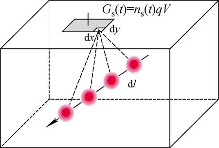
Fig.1 Spherical diffusion charge collection model for sensitive nodes under fixed bias
As introduced before, the charge collection process dynamically interacts with the circuit response. The transient pulse is shaped by the potential collapse of the p-n junction and the surrounding circuitry’s driving ability. The rebuilt SET waveformGs(t) is used as the kernel function in the bias-dependent model as shown in Fig.2. The circuit response effect is reflected by the bias-dependent calculator.Csis the inner capacitance of sensitive node.Gr(t) is the recombination current due to the circuit response. Output currentGSEE(t) is connected with the transistor internal junction nodes (p-type and n-type). The calculation of dependent current sourceGr(t) andGSEE(t) uses the Verilog-AMS behavioral modeling language as a system of equations[14]:
Gr(t)=f(V(Cs),Cs,RcombParameter)
GSEE(t)=f(V(Cs),Cs)×Fermi(V(p,n))
(6)
The Fermi-style function is used to clamp theGSEEwhen the junction is forward:
(7)
TheFparameter determines the junction bias range and is set to 0.01 in this paper.

Fig.2 Equivalent bias-dependent current calculator inserted into transistor BSIM model[6]
Fig.3 shows the schematic representation of radiation sub-circuit for single spot strike. The well potential modulation effect of the SE-related currents for the hit nodes is calculated by the current sourceIwellflowing through the resistance network between N well and P well. The transistor body potential change controls the turn-on of parasitic bipolar transistor. The current gain was set 1.5 for PMOS in 65 nm technology. In previous work we have shown the measurement method of well spreading resistance and well contact resistance[15].

Fig.3 Schematic representation of SE sub-circuit with resistance network for single spot strike
Rcontrepresents the well contact resistance, andRwellandRbsrepresent the well spreading resistance.

Fig.4 Single-event characterization flow integrated into custom EDA design flow
The SEE simulation process is shown as Fig.4. Our tool is integrated into the standard EDA design flow by inserting the radiation sub-circuit into the netlist. Our approach can obtain SEU cross section using SPICE simulations with some TCAD calibrations and layout information analysis. The required data are the calibrated parameters and PDK information. This tool could help designers to estimate quickly the fault tolerance parameters of the designed cell.
3 Test chip and simulation result
The test chip M328C is non-radiation hardened 6T cell SRAM. The test block involves 16 cells with one cell area 1.05 μm×0.5 μm as shown in Fig.5. Bit interleaving is used in all SRAM blocks, and the successive bits in the same logical word are physically separated by inserting bits of other 15 logical words. The chip was written with 55H pattern the same with experiment. The sensitive nodes are identified in Fig.4. Vertical and tilting 60° incidences along the well were performed during both simulation and experiment. In our model there are some basic assumptions for single spot strike.

Fig.5 Layout schematic of 16 cells SRAM block
1) The layout was meshed into 0.1 μm×0.1 μm boxes. The single spot strike location is in the center of the box. The bit cross section is the sum of flipped box area.
2) According to Ref. [16], charge sharing between N well and P well is insignificant. When ions strike P well region only the NMOS transistors are affected, and respectively for PMOS.
The model parameters should be calibrated to 3D TCAD simulation results for different LET values. We built the 3D TCAD structure for 65 nm technology. The drain contact is under fixed bias during simulation. Table 1 shows the technology dependent model parameters which are extracted for cases of shared charge being collected by multiple devices. Ions strike with higher LET will deposit larger number of excess carriers in well which changes the doping level under the junction node instantaneously. As the LET value increases, the diffusion constantDαincreases as well which broadens the pulse width of the calculated waveforms.

Table 1 65 nm technology model parameter calibrated by 3D TCAD
Fig.6 shows the comparison of the bit-upset cross section simulation results with the experiments for 6T SRAM block. The LET values of ions in experiment are recalculated considering the multiple metallization. Test data in experiment at normal incidence are fit with Weibull function. SEU saturation cross section is 1.85 μm2at normal incidence. The cross section value is over three times more than one cell size, indicating very serious MCU effects[17]The simulation results for normal and tilt incidence are also shown in this figure with red dot. The effective LET value is 10 MeV·cm2/mg and 30 MeV·cm2/mg for normal strike. The cross section curve and multiplicity distribution map are shown in Fig.6 and Fig.7. It is important to note that we consider only the diffusion mechanism when calculating the collected charges. The drift current induced by the potential collapse in the drain and well junction is short and burst and is neglected in our model. In low LET case, the field driven charge collection also takes contributions to the total error cross section, which explains the lower simulation results. At high LET the carriers concentrations exceed the well and substrate doping levels several tens of picoseconds after the strike. The carrier lifetimeτin well region during the whole collection process should decrease due to the enhanced recombination process. Otherwise, the ambipolar diffusionDαvaries versus time during the whole collection process.Dαis related to the carrier mobility and the degradation of mobility is due to the carrier-carrier scattering. Assuming thatτandDαare constant introduces systematic error and overestimates the amount of charge injected at high LETs.
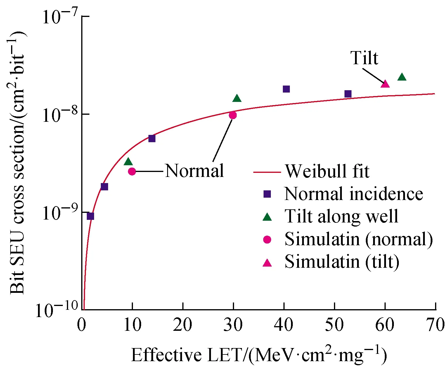
Fig.6 Comparison of simulation result with experiment for 6T SRAM block

a—LET=30 MeV·cm2/mg, normal strike;b—Effective LET=60 MeV·cm2/mg, following the 1/cos lawFig.7 Contribution of SCU and MCU in total cross section (red square indicating cell under test)
4 Conclusion
We present a circuit-level modeling tool integrated into the standard EDA flow. Two dominating processes of charge sharing (diffusion and bipolar effect) are considered and well modeled by an engineering approach. Most of the parameters are physics-based. Instead of traditional 1/cos law, we use the three-dimensional spherical diffusion model to rebuild the current waveform for angular strike. The proposed tool is useful for designers to estimate the vulnerability of unit circuit.
- 原子能科学技术的其它文章
- H-1NF仿星器标准磁场位形分析与高能量离子运动轨道模拟
- 铀转化生产线含氟废水处理工艺设计
- 在线进样ICP-MS用于239Pu气溶胶活度浓度连续监测技术研究
- Degradation Characteristic of Proton Irradiated 8T CMOS Image Sensor
- Comparative Experimental Study on Space Electrostatic Discharge Effect and Single Event Effect of 130 nm SOI D Flip-flop Chains
- Effects of Electron Irradiation at Different Energy and Fluences on Electrical Properties of InP HEMT Structure