
Radiation-induced Dark Current Random Telegraph Signal on CMOS Image Sensor
2021-12-15 14:35LIUBingkaiLIYudongWENLinZHOUDongGUOQi
原子能科学技术 2021年12期
LIU Bingkai, LI Yudong, WEN Lin, ZHOU Dong, GUO Qi
(1.Key Laboratory of Functional Materials and Devices for Special Environments, Chinese Academy of Sciences, Urumqi 830011, China; 2.Xinjiang Technical Institute of Physics and Chemistry, Chinese Academy of Sciences, Urumqi 830011, China; 3.Xinjiang Key Laboratory of Electronic Information Material and Device, Urumqi 830011, China; 4.University of Chinese Academy of Sciences, Beijing 100049, China)
Abstract: Radiation damage causes the dark current random telegraph signal (DC-RTS) on CMOS image sensors used for space and nuclear applications. Several 0.18 μm CMOS image sensors were irradiated by distinct proton energy and gamma rays, and the characteristic parameters of DC-RTS were analyzed after irradiation. Experimental results show that there are discrepancies between DC-RTS pixels due to displacement damage and to total ionizing dose effects in terms of discrete level, maximum transition amplitude and average time. This is because both kinds of radiation damage induced RTS defects are different. Contrary to the DC-RTS due to displacement damage, total ionizing dose induced DC-RTS features small transition amplitude and low transition frequency, which gives rise to the test and analysis challenge for this DC-RTS. Transfer gate voltage during integration has an important impact on total ionizing dose induced DC-RTS. The above work provides an important reference for the better understanding of DC-RTS phenomenon on CMOS image sensor, and the exploration of relevant suppression techniques.
Key words:CMOS image sensor; displacement damage effect; total ionizing dose effect; dark current random telegraph signal
1 Introduction
CMOS image sensors (CIS) as the core imaging device are widely used in space imaging and nuclear industry missions[1-2]. The CIS used for the above applications are exposed to harsh radiation environment and the particles (protons, electrons and heavy ions) cause various radiation effects including total ionizing dose (TID), displacement damage (DD) and single event effects (SEE)[3-4]. Among these radiation effects, TID and DD are the cumulative radiation effects. TID induces oxide charges and interface states in the dielectrics and both kinds of defects lead to the degradation of the key parameters. DD produces bulk defects at the space charge region (SCR), and introduces the energy level within the Si bandgap. The bulk defects play as recombination-generation centers and limit the performance of the CIS. TID and DD generate dark current random telegraph signal (DC-RTS) in the pinned photodiode (PPD) of the CIS. DC-RTS refers to the random fluctuations of dark current output with time between two or more discrete levels and has an influence on in-flight calibration of the dark current.
In 1993, Hopkinson et al.[5]firstly reported the DC-RTS phenomenon in proton-irradiated CCD. In the past 30 years, many researchers have carried out a series of studies on DC-RTS[6-10]. Research topics mainly focus on: optimizing RTS software to improve the detection efficiency of DC-RTS; establishing physical model to predict the occurrence probability of DD-induced DC-RTS (DDD-RTS); the first report of TID-induced DC-RTS (TID-RTS), which breaks the inherent understanding that only DD can produce DC-RTS; exploring the influence of annealing temperature on DC-RTS behavior; and investigating the effects of radiation and technology parameters on DC-RTS. In these published literatures, more efforts are made in improving the understanding of DDD-RTS, but few papers focus on TID-RTS[11-12]. This is because TID-RTS exhibits fluctuation characteristics different from the DDD-RTS, which brings challenges to the test and analysis of TID-RTS.
The purpose of this paper is to obtain the comprehensive understanding of radiation-induced DC-RTS. Firstly, the main characteristics of the studied CIS and the experimental details are introduced. Then the results of DC-RTS after exposure to proton and γ rays are presented and the behaviors of both kinds of DC-RTS are compared. Finally, the influence of transfer gate (TG) voltage during integration on TID-RTS is analyzed.
2 Experimental detail
2.1 Device information
The devices under study are the 0.18 μm CIS. The sensor consists of 2048×2048-11 μm-pitch pixels. The pixel scheme is the 4T PPD as detailed in Fig.1. Apart from the PPD, it includes a reset transistor, a TG tran-sistor, a source follower transistor and a row select transistor. The CIS integrates a 12-bit ADC, a temperature sensor, a phase locked loop and serial peripheral interface control on chip. The pixel is electrically and optically isolated by a shallow trench isolation (STI) structure. All the CIS used in this work are from the same lot.

Fig.1 Schematic of 4T pixel
2.2 Irradiation experiment
The proton irradiation experiments were performed at the cyclotron accelerator (at China Institute of Atomic Energy, Beijing, CHN) with the energy of 50, 60 and 70 MeV. The proton fluence rate is 5×106cm-2·s-1. The used image sensor applies the pin grid array (PGA) package, and it is unnecessary to decap the device since proton range is enough to reach the SCR. The γ irradiation experiments were carried out at60Co-γ radiation source (at Xinjiang Technical Institute of Physics and Chemistry, Urumqi, CHN). Dose rate was set to 50 rad(Si)/s and the maximum dose is 50 krad(Si). All the irradiation experiments were carried out at room temperature and the CIS was unbiased with all pins grounded during irradiation. Irradiation experiment details are shown in Table 1.
Table 1 Irradiation experiment detail
2.3 DC-RTS test
Proton-irradiated CIS is used to study DDD-RTS and γ-irradiated CIS for TID-RTS. DC-RTS test was carried out at 24 ℃ after irradiation. The test chamber has air-conditioning to control the measurement temperature. The raw images were successively grabbed by a data acquisition software at the frequency of 2 s per frame, and the integration time was set to 0.2 s during image acquisition. Except for the considerations mentioned above, other issues are VLOTG and test duration. VLOTG corresponds to the TG voltage during integration and the voltage has an impact on TG channel regime (accumulation or depletion). For DDD-RTS, the VLOTG was set to -0.2 V to exclude the contribution of TG oxide to DC-RTS and the test duration is 2 hours. As for TID-RTS, the VLOTG options include -0.2 V, 0 V and 0.2 V to investigate the influence of TG oxide on the DC-RTS and the image acquisition duration is 5 hours. To reduce the pressure of data storage and analysis caused by long-term image acquisition, the windowing operation mode was applied during image acquisition. After test, RTS software, which is implemented using Matlab software, is used to automatically detect the DC-RTS pixels on a subarray and extract the characteristic parameters including DC-RTS pixel count, discrete level, maximum transition amplitude and average time.
3 Result and discussion
3.1 DDD-RTS characteristic
The definition of the characteristic parameters of DC-RTS is presented in Fig.2. Each dark current value corresponds to a DC-RTS level, and the minimum dark current is defined as the first level. Dark current difference between levels is the transition amplitude and the maximum difference among all the transition amplitudes is the maximum transition amplitude. The average of all the retention time at a given level is defined the average time specific to this level.
DDD-RTS level distributions are shown in Fig.3. It can be seen that the number of 2-level DC-RTS accounts for 60% of the total DDD-RTS pixels, and the highest level is 8. DDD-RTS is the result of the proton-induced metastable bulk defects at the SCR. Metastable defects feature two or more configurations, each of which corresponds to a generation rate. DC-RTS phenomenon is observed when the metastable defect randomly jumps between the generation rates. DC-RTS level represents the structural information of metastable defects. 2-level DC-RTS is caused by a metastable defect containing two configurations (called bistable defect). The generation mechanism of multilevel DC-RTS is complex and there are two possible physical explanations. The first hypothesis supports that multilevel DC-RTS is due to a metastable defect featuring multiple configurations (called multi-stable defect). The other hypothesis thinks that multilevel DC-RTS is the result of the combination of several bistable defects.

Fig.3 DDD-RTS pixel level distribution

f(x)=k/λ·exp(-x/λ)
(1)
Wherekis determined byy-intercept,λis the average of the exponential law, andxis the transition maximum amplitudes. From Fig.4, one can see that the average of exponential law is 1100 e-/s, and the value is same for the considered proton energy. This suggests thatλis a characteristic value dependent on the radiation effect type.
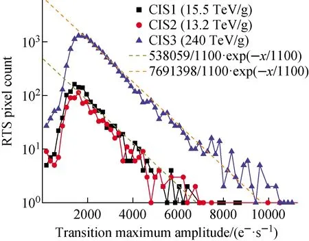
Fig.4 DDD-RTS transition maximum amplitude and fitting using exponential function
Fig.5 depicts the fluctuation trace of 2-level DDD-RTS. There are obvious differences in transition frequency for these DDD-RTS pixels. In order to quantify the transition fre-quency, the average time of DC-RTS is calculated as detailed in Table 2. The mean value of average time for the first level is 64 s, and the one for the second level is 131 s. Transition from first level to second level is more frequent than from second level to first level, which indicates that there is a higher potential barrier when metastable defect jump from the second level to first level. Moreover, transition frequency for DDD-RTS is approximately 10-2s-1at 24 ℃. Such a frequent transition suggests that more concern should be taken in DDD-RTS when calibrating the dark current in orbit.

Fig.5 Examples of typical 2-level DDD-RTS pixels

Table 2 Average time at distinct discrete levels for DDD-RTS pixel
3.2 TID-RTS characteristic
It is well known that the sensitive region of DD effect is the SCR and thus fabrication process dependence of DDD-RTS is weak. As for TID-RTS, sensitive region is the depleted-Si/SiO2. There are several sources of depleted-Si/SiO2in a 4T PPD pixel, such as STI, pre-metal dielectric (PMD) and TG oxide. Unlike STI and PMD dependent on the fabrication process and pixel design, the influence of TG oxide on TID response depends on the operation mode of the CIS. For this, the VLOTG should be carefully chosen. When TG channel is in the accumulation regime, the electrons of the saturated pixel (such as hot pixel) can not be collected by the float node due to the existence of high potential barrier. These electrons are collected by the adjacent pixel through the epitaxial layer with a relatively low doping concentration, which causes the dark current blooming effects and seriously affects the image quality. When TG channel is in the depletion regime, dark electrons due to the interface states of TG oxide are collected effectively by SCR and thus total dark current significantly increases, which leads to the increase of dark current shot noise and the drop of sensitivity.
The influence of VLOTG on TID-RTS is shown in Fig.6. Compared to the DDD-RTS, TID-RTS is caused by the metastable interface states. VLOTG of -0.2 V and 0.2 V corresponds to accumulation and depletion regime of the TG channel, respectively. When TG channel is in the depletion regime, the number of TID-RTS significantly increases since more metastable interface states of TG oxide become active. It can be seen fro Fig.6a that 2-level DC-RTS accounts for 90% of total TID-RTS and the highest level is 5. This suggests that γ ray produces a large number of bistable interface states, and the structure of metastable interface states is simpler than the metastable bulk defects. From >Fig.6b, one can see that the transition maximum amplitude of TID-RTS has same slope under distinct VLOTG, and the average of the exponential law is 110 e-/s, which is much smaller than that of DDD-RTS. Such a small transition amplitude brings a challenge to the TID-RTS test, that is, RTS software is able to accurately identify slight transition without the misjudgment of TID-RTS.

Fig.6 TID-RTS pixel level (a) and transition maximum amplitude (b) under different VLOTGs

Fig.7 Examples of typical 2-level TID-RTS pixel
Fig.7 depicts the fluctuation trace of 2-level TID-RTS. Apart from the RTS#3 and #8, other RTS pixels exhibit low transition frequency during 5 hours observation time. The results of average time of TID-RTS are presented in Table 3. The mean value of average time for the first level is 1519 s, and the one for the second level is 1745 s. The transition frequency of TID-RTS is around 10-3s-1, which is much smaller than that of DDD-RTS. To obtain enough jumps, long-term test is required for the TID-RTS, which brings another challenge, such as data storage and analysis.
3.3 DC-RTS defect concentration
As discussed above, the defects responsible for RTS behavior are the metastable defects. RTS defect concentration is determined according to the calculation method from Ref.[8].Fig.8 depicts the metastable bulk defect concentration as a function of DDD. It is shown that metastable bulk defect concentration linearly increases with DDD at the considered DDD range. RTS factor (KRTS) represents the occurrence of RTS defects per unit volume and per unit DDD (corresponding to the slope of the curve). In our work,KRTSis 30 Def·cm-3·(MeV/g)-1and this value is independent on particle energy and radiation fluence. This means that RTS defects concentration can be predicted with the determination of the volume of SCR and the absorbed dose.Fig.9 shows metastable interface state concentration at 50 krad(Si) for several VLOTGs. Metastable interface state concentration is the order of 107cm-2at the considered TID range. And RTS defect concentration significantly increases when the TG transistor is in the further depletion regime (corresponding to 0.2 V). This suggests that TG gate oxide is an important source of TID-RTS and the depletion regime should be avoided in the TID-rich applications.
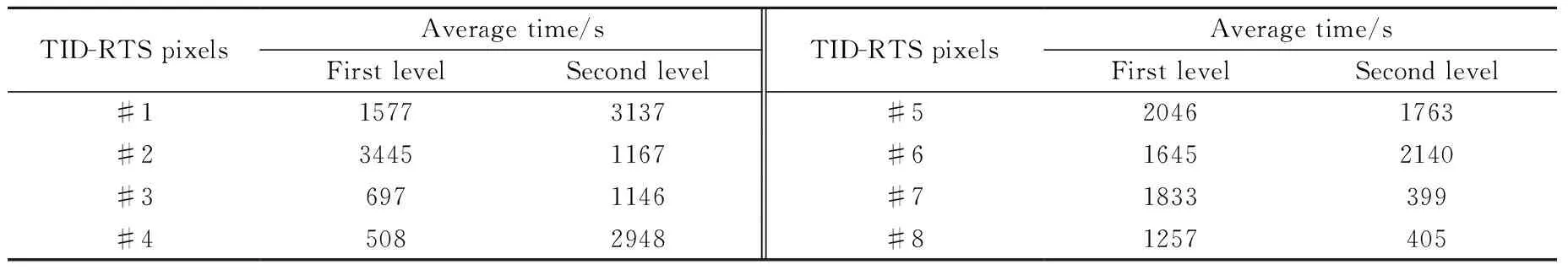
Table 3 Average time at distinct discrete levels for TID-RTS pixel

Fig.8 Metastable bulk defect concentration as a function of DDD

Fig.9 Metastable interface state concentration at 50 krad(Si) for several VLOTGs
4 Conclusion
Several 0.18 μm 4T PPD CIS were irradiated by proton and γ rays to investigate the radiation-induced DC-RTS. The difference between TID-RTS and DDD-RTS is analyzed through the comparison of characteristic parameters including DC-RTS pixel count, discrete level, maximum transition amplitude and average time. The experimental results are as follows.
1) After irradiation, a large number of DC-RTS is 2-level, regardless of radiation damage types. The percentage of multilevel DDD-RTS is larger than that of multilevel TID-RTS. This suggests that proton-induced metastable bulk defects are more complex than metastable interface states produced by γ rays.
2) Maximum transition amplitude distributions of two kinds of DC-RTS feature same shape and it is composed of Gaussian peak and exponential tail. The average of exponential function is a useful tool to distinguish DDD-RTS from TID-RTS. The average of exponential law for DDD-RTS is 1100 e-/s,while the one for TID-RTS is 110 e-/s. Small transition amplitude brings a challenge to TID-RTS test, such as the ability of RTS software.
3) Average time reflects the stability of RTS defect at a discrete level. At room temperature, the transition frequency of DDD-RTS is about 10-2s-1, and the one for TID-RTS is around 10-3s-1. This discrepancy in transition frequency shows that DDD-RTS have an important influence on in-orbit dark current calibration compared to TID-RTS. Low transition frequency brings another challenge to TID-RTS test, that is, data storage and analysis due to a long-term test.
4) At the considered DDD range, metastable bulk defect concentration linearly increases with DDD. AndKRTSis 30 Def·cm-3·(MeV/g)-1in our work. In a 4T PPD pixel, there are several sources of TID-RTS, such as STI, PMD and TG oxide. Among these sources, the contribution of TG gate oxide can be decreased effectively by VLOTG. When the TG channel is in the depletion regime, metastable interface state concentration reaches the order of 108cm-2and this case should be avoided in the TID-rich applications.
- 原子能科学技术的其它文章
- H-1NF仿星器标准磁场位形分析与高能量离子运动轨道模拟
- 铀转化生产线含氟废水处理工艺设计
- 在线进样ICP-MS用于239Pu气溶胶活度浓度连续监测技术研究
- Degradation Characteristic of Proton Irradiated 8T CMOS Image Sensor
- Comparative Experimental Study on Space Electrostatic Discharge Effect and Single Event Effect of 130 nm SOI D Flip-flop Chains
- Effects of Electron Irradiation at Different Energy and Fluences on Electrical Properties of InP HEMT Structure