
Design of broadband achromatic metasurface device based on phase-change material Ge2Sb2Te5
2022-12-28 09:53ShuyuanLv吕淑媛XinhuiLi李新慧WenfengLuo罗文峰andJieJia贾洁
Chinese Physics B 2022年12期
关键词:文峰
Shuyuan Lv(吕淑媛), Xinhui Li(李新慧), Wenfeng Luo(罗文峰), and Jie Jia(贾洁)
Xi’an University of Posts&Telecommunications,School of Electronic Engineering,Xi’an 710121,China
Keywords: metasurface,optical device,phase-change material,achromatic
1. Introduction
So far, transmission-type[1,2]and reflection-type[3,4]metasurface devices have gradually replaced bulky and huge traditional optics devices, due to the compact and easy-tomanufacture characteristics, as well as for flexible and effective control of electromagnetic wave polarization, amplitude,phase,and propagation mode,[5–11]by adjusting the geometric parameters of the nanopillar. With these advantages, metasurface devices are extensively used in such fields as invisibility cloaks,[12]high-dimensional holograms,[13,14]ultra-thin metalenses,[15–19]and vortex beams.[20,21]At the same time,metasurface devices have obvious dispersion problems mainly due to the intrinsic dispersion of the material itself. Intrinsic dispersion is caused by many factors,like the resonance phase of the metasurface nanopillars,different refractive index at different wavelengths and the difference of the propagation phase in free space,which leads to the decline of imaging quality. In a word,it is still a major challenge to realize achromatic metasurface devices.
In order to solve the chromatic aberration problem, researchers used different methods to realize various achromatic devices based on different materials. For instance, in 2017,Wang Shuminget al.[22]used Au as a nanopillar unit,SiO2/Au as a substrate, designed a metasurface integration unit with smooth linear phase dispersion, and combined with geometric phase to achieve broadband achromatic optics device. It is proved that the designed metalenses and beam deflector metasurface can achieve achromatic effect within the near-infrared waveband of 1.2 µm–1.68 µm. In 2018, Sajan Shresthaet al.[23]used positive squares, hollow squares, concentric squares, cross-positive squares, and inner-cut squares to increase the dispersion of the metasurface, resulting in higher passivity of nanopillar.In the transmission mode,polarizationindependent achromatic devices can be realized in the nearinfrared waveband 1.2 µm–1.65 µm, and the focusing efficiency can reach 50%. This method is an important step in the practical application of metalens.
In recent years, the unique characteristics of the phasechange materials have been developed by researchers and achromatic metasurface devices have been implemented with phase-change material. With appropriate stimulation of light, electricity or temperature, the phase-changing material can alter between the crystalline state and the amorphous state. Optical devices, like optical switch and achromatic metalenses,[24–26]have been realized based on these phasechanging material. In 2020, Ding Xiyaet al.[26]proposed a chromatic aberration compensation metasurface scheme based on phase-changing materials, and designed corresponding achromatic metalenses and beam deflector metasurface within the continuous waveband 8 µm–11 µm by uniformly adjusting the crystallization fraction of the phase-change material Ge2Sb2Te5(GST). This literature used the incident wavelength of 8.5µm as the basic wavelength, and the size of the nanopillars is obtained by scanning when the phase-change material crystal fractionmis 0.6.Finally,the achromatic function of the metasurface device was realized by adjusting the crystalline fraction of the phase-change material.
Combined with the design method in this article, the phase-change material GST is selected as the material of the nanopillar,because it has the characteristics of obvious phase change, significant refractive index change between amorphous and crystalline states,and fast switching speed.[27]Both crystalline and amorphous states in the longer-infrared band have low absorptivity, which makes it possible to achieve achromatic design in the longer-infrared band. In this article,the corresponding phase is obtained by changing the radius of the nanopillars,so linearly polarized light is used as thexpolarization state to realize the achromatic function.
In order to realize a wider bandwidth of achromatic metasurface optical device, a lot of work needs to be done on the resonant unit. In this article,we use the linear phase gradient combined with the crystalline fraction of the phase-changing material GST to design an achromatic metasurface optical device within the continuous wavelength range of 9.5 µm–13 µm. Simulation results demonstrated that this achromic metalenses is well realized with focus to the same focal plane in the working waveband,and the diffraction limit is reached.In addition, to further demonstrate the practicability of this method, the method is used to realize a beam deflector metasurface with a deflection angle of 19◦in the working waveband. Our study not only provides a way to the realization of broadband achromatic metasurface, but also has potential application in fields,like communication technology,medical equipment,and holographic technology,and so on.
2. Design principles and method
Two types of metasurface devices, a transmissive achromatic metalenses and a beam deflector metasurface with the same deflection angle, are designed by the phase-change material GST. The working wavelength is 9.5 µm–13 µm, and the minimum wavelength is 9.5 µm used as the basic wavelength. The basic unit structure of the device consists of two parts shown in Figs. 1(a) and 1(b). The top part of the unit consists of concentric solid and hollow cylindrical nanopillar with the high refractive index material of GST.The substrate is CaF2with low refractive index of 1.34. The near-field distributions of these two structures are shown in Figs. 1(c) and 1(d), and both nanopillars support the waveguide cavity resonance. Whenh=6.5 µm, it can be seen that the phases of both nanopillars cover 0–2π.
Periodic boundary conditions are used in thexandydirections,perfect matching layer(PML)is used in thezdirection, and the thickness of the PML is set to 2π/k0, wherek0is the wave vector in vacuum. The periodsPxandPyof the basic unit are set to be 2.3µm in order to satisfy the Nyquist sampling lawP<λ/2NA,whereλis the wavelength andNAis the numerical aperture with the value of 0.584.
In order to achieve high-efficiency and wide-bandwidth achromatic metasurface devices, two types of nanopillars are used in this article,as shown in Fig.1.The device is composed of solid cylinders and hollow cylinders of different diameters,through the combination of linear phase gradient and phasechange material fraction to realize an achromatic metasurface device.

Fig. 1. (a) Front view of nanopillars unit. (b) Top view of nanopillars unit. Solid nanopillar is GST with height h and radius r1. Hollow nanopillar have outer radius r2 and inner radius r3, and the substrate is CaF2. (c) The near-field image of a hollow cylinder, r2 =0.96 µm,r3=0.4µm,λ =9.5µm. (d)The near-field image of a solid cylinder,r1=0.88µm,λ =9.5µm.
At the operating wavelength, the phase distribution formula required by the achromatic device is

wherecandfare the speed and frequency in vacuum, respectively,Frepresents the focal length of the metalenses,and (x,y) are the position coordinates of the lens unit in the plane lens. In order to realize the achromatic metalenses, an additional phase shift is introduced shown in Fig. 2, and the corresponding formula is written as

whereϕshift(f)is a reference phase function that has nothing to do with (x,y). After interacting with the metalens, only the spatial phase difference has an effect on the focal point of the lens. So we only need to consider the phase shift, that is,when (x,y)=0, the phase difference between the phase and the reference phase(9.5µm). And the phase shift distribution equation of the vertically incident wave is

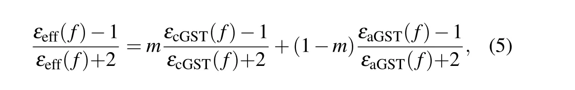
wherem(x,y)is the slope of the phase shift frequency. From Eqs. (3) and (4), it is concluded that the phase shift of the broadband achromatic metalenses at all positions has a linear relationship with frequency. In this work, hollow cylinders and solid cylinders are used as nanopillars to increase the dispersion of nanopillars. Since the phase distribution of each wavelength is completely independent, each GST nanopillar unit should provide a unique phase response. Each nanopillar is designed by changing the diameterr1of the cylinder and the diametersr2andr3of the hollow cylinder. Therefore,this work uses the linear phase gradients dispersion of the nanopillar to realize the achromatic device of 9.5µm–13µm,as shown in Fig.3(a). The size and shape of its 12 nanopillars are shown in Table 1.

Fig.2. Phase distribution of wide-band achromatic metalenses at working wavelengths.
Figure 3(a) shows the linear relationship with 12 GST nanopillars as a representative. The slope from unit 1 to unit 7 increases, but the slope from unit 8 to unit 12 decreases slightly compared to unit 1 and unit 7. Considering the problem of craftsmanship, the size of the hollow and solid cylinders selected in this article cannot be accurate to 1 nm,so the size searched by the slope cannot be a perfect match. There is a certain deviation, and the achromatic effect cannot reach the ideal state. Therefore, a wider achromatic effect can be achieved by adjusting the crystalline fractionmof the phasechange material.

Table 1. Data of dimensions of unit structures.
Figure 3(b) is a metalenses composed of 49 GST solid cylinders and hollow cylinders. Since metalenses are symmetrically arranged in the simulation design,there are 25 nanopillars in the designed metalenses a linear relationship. And Fig. 3(b) shows that there is still chromatic aberration within the bandwidth of 9.5 µm–13 µm, and it can be seen that the larger the wavelength,the more the derivative focus.
In addition, the unique properties of the phase-change material are also used to increase the working bandwidth of the achromatic metalenses by the adjustment of crystalline fraction of the phase-change material. The dielectric constant of GST under different crystalline fraction conditions can be realized by the effective medium theory. The Lorentz–Lorenz[28]relationship is used to define the crystalline fraction formula of GST as
whereεaGSTandεcGSTare the dielectric constants related to the frequency of crystalline and amorphous GST, respectively. The dielectric constant of the phase-change material is obtained from the literature.[29]mis the crystalline fraction,ranging from 0 (amorphous) to 1 (crystalline). In this work,the refractive index of GST in the amorphous and crystalline states is used within the waveband of 9.5µm–13µm,and the corresponding refractive index varies from 4.27 (amorphous state) to 6.3 (crystalline state). The simulation result of the metalenses designed by the change of themvalue of GST is shown in Fig.4.
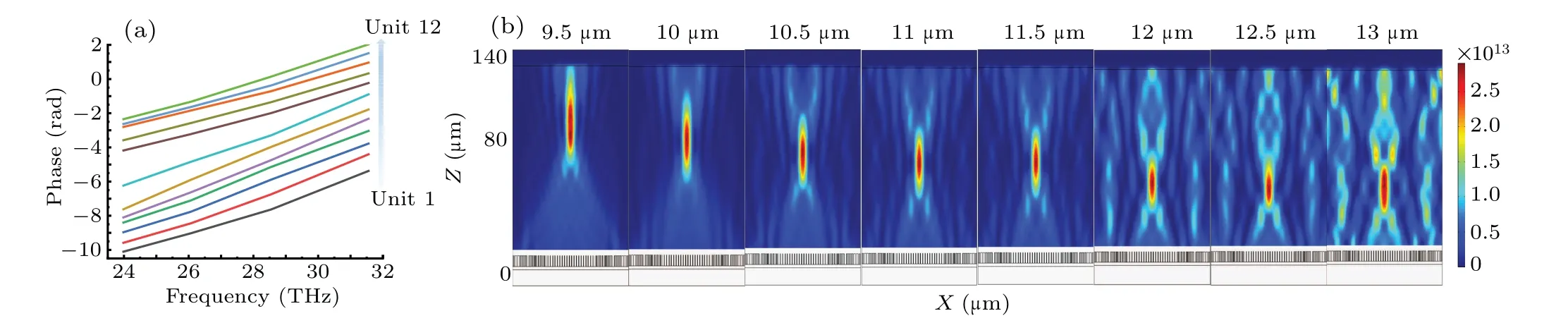
Fig.3. (a)The output phase of some unit selected in the metalenses varies with frequency. (b)Distribution of the electric field intensity of the metalenses at each wavelength.

Fig.4. The m-tuned achromatic metalenses. By adjusting the crystalline fraction m of the phase-change material, the distribution of electric field intensity of achromatic metalens is studied.
In the experiment, the pulse energy can be controlled by the local heating of femtosecond laser pulses.[30]The crystallization fraction of GST is adjusted by the pulse energy after heating, so as to achieve the achromatic effect of the phasechange material.[31,32]
The metalenses are designed with the size of GST nanopillars at 9.5µm. The types of nanopillars used are solid cylinders. After simulation calculation, only by adjusting the crystalline fractionmvalue of the phase-change material, the achromatic effect will be achieved in the wavelength range of 9.5 µm–10.5 µm, when the wavelength is greater than 10.5 µm, the focal length is significantly reduced, so further adjustment and optimization are still needed to realize achromatic lenses in a larger wavelength range.
3. Results and discussion
Without any phase compensation, the result of incident wave is shown in Fig.5(a). The focal length decreases as the incident wavelength increases, which is due to the inherent chromatic aberration of the material. If the cell size data is only found by the slope of the relationship between the phase and frequency, the achromatic bandwidth of the metalens is limited. In addition, due to the variable characteristics of the phase-change material between the crystalline and the amorphous, the metalens can exhibit a certain achromatic effect.The simulation result of only adjusting the crystalline fractionmof the phase-change material is shown in Fig.4. Although there is achromatic effect, the achromatic effect is not ideal,and the wavelength range is small.
Therefore, two methods are combined together to compensate for the chromatic aberration and realize the achromatic metasurface device. Firstly, hollow cylinders and solid cylinders are chosen as nanopillars and their sizes are selected according to the linear relationship between phase and frequency. However, considering the problem of craftsmanship,some practical sizes of the nanopillars do not match the required sizes. Therefore, the achromatic effect can be realized only within the small bandwidth. In order to realize the achromatic device with a larger bandwidth, we can change the refractive index of the phase-change material between the crystalline and the amorphous, and the achromatic effect can be realized correspondingly. With the combination of these two methods,the achromatic effect of the metalens with larger bandwidth is realized.
Through simulation calculations,this method realizes an achromatic metalenses with a larger bandwidth,increasing the original bandwidth of 9.5µm–10.5µm to 9.5µm–13µm,with the increase of the bandwidth of 2.5µm.The electric field distribution in itsx–zplane is shown in Fig.5(b),the focal lengthf=80µm remains almost unchanged,and the result is as expected. The relationship between the achromatic focal length and the incident wavelength is shown in Fig. 5(c). The focal length oscillates at 80µm in the bandwidth of the incident wavelength from 9.5 µm to 13 µm, and it shows that the designed achromatic metalens is feasible.
The corresponding FWHMs are 7.428 µm, 7.442 µm,7.231 µm, 7.338 µm, 8.074 µm, 8.737 µm, 8.742 µm, and 9.122µm,respectively. According to the diffraction limit formula FWHMlim=λ/2NA,whereλis the incident wavelength andNAis the numerical aperture of 0.584,and the calculation results show that the FWHM of the metalenses are close to the diffraction limit. The wavelength dependence of the FWHM spot size and focusing efficiency is shown in Fig.5(d). It can be seen from the figure that the focusing efficiency is above 60%. It is proved that the achromatic metalens designed in this article has a good focusing effect.

Fig. 5. (a) Chromatic metalenses. The distribution of electric field intensity at each wavelength using a metalenses designed with a solid cylinder at λ =9.5 µm. (b) Achromatic metalenses. The distribution of electric field intensity of achromatic metalenses at each wavelength and its FWHM distribution at each wavelength. (c)The relationship between wavelength and focal length. (d)The relationship between FWHM,focusing efficiency and wavelength.
In addition, Table 2 summarizes some of the work on achromatic metalenses, comparing materials, working bands,and focusing efficiency. Compared with literature,[18,22,26]the achromatic metalens designed in this paper not only has a larger working bandwidth,but also has a higher focusing efficiency. Moreover,the achromatic method used in this paper is relatively novel,which brings new ideas for the realization of achromatic lenses with larger bandwidth in the future.
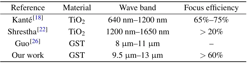
Table 2. Comparison of the work in this article and other work of the same type.
An achromatic beam deflector metasurface with the same deflection angle is also designed and analyzed with the combination of these two methods mentioned above. According to the generalized Snell’s law, the phase gradient distribution formula of the achromatic beam deflector metasurface is designed as

whereλis the incident wavelength,θ1andθ2are the incident angle and refraction angle,andn1andn2the refractive indices of the incident medium and output medium, respectively. In the air with normal incidence,the generalized Snell’s law can be rewritten as
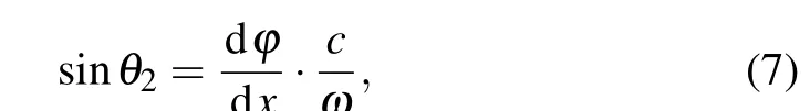
whereωrepresents the angular frequency, andcrepresents the speed of light in vacuum. The term dϕ/dxrepresents the phase gradient required to guide the beam to a certain angle at a certain frequency,and there should be a certain linear relationship between the phase gradientϕand the positionxof the beam deflector along the air–metasurface interface. Therefore,the relationship between the required transmission phase of the unit and its positionxand angular frequencyωcan be written as the following formula:

In order to construct the beam deflector with the same refractive angle at different frequencies,the nanopillar unit needs to satisfy the linear dispersion dϕ/dω,which can be obtained by changing the radius of the nanopillars to control the dispersion shown in Fig.6(a).
In this work, the deflection angle 19◦of the achromatic beam deflector metasurface is designed by combining the linear phase gradients with the crystalline fractionmvalue of the GST. In order to satisfy the linear relationship between the phase and frequency of each nanopillar within the designed waveband, the phase difference is ∆ϕ=π/6 with the incident wavelength 9.5µm,and ∆ϕ=2π/15 with 12.5µm. Figure 6(b)shows that the deflection angle of the designed beam deflector at 9.5µm wavelength is 19◦,which has obvious chromatic aberration in the working waveband. Through the individual design of the nanopillar unit and the calculation of themvalue of the phase-change material, the achromatic beam deflector metasurface is realized with the incident at wavelengths of 9.5µm,10µm,10.5µm,11µm,11.5µm,12µm,12.5µm,and 13µm,and the corresponding crystal fractionmare 0,0,0,0,0,0.3,0.5,and 0.7,respectively. And the deflection angles are 19.35◦,19.05◦,19.89◦,19.98◦,19.61◦,20.07◦,20.24◦, and 21.25◦, respectively, which are all within the acceptable error range. In addition,it can also be seen from the output electric field diagram of the deflector in Fig. 7(a) that the deflection angle is about 19◦. The functional relationship between the transmission field strength, deflection angle and wavelength of the achromatic deflector is shown in Fig.7(b).
Fig.6.(a)The output phase of some unit selected in the beam deflector metasurface varies with frequency.(b)Chromatic beam deflector.Beam deflector designed with a hollow cylinder is used atλ=9.5µm,and its deflection angle changes with the increase of wavelength,and there is obvious chromatic aberration. (c)Achromatic beam deflector metasurface. After optimization,the beam deflector metasurface deflection angle is almost unchanged,which is about 19◦.
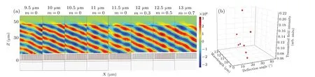
Fig.7. (a)Output electric field diagram at each wavelength. (b)3D plot of transmitted field strength versus deflection angle,incident wavelength.
4. Conclusion
This article proposes and simulates an achromatic metalenses and beam deflector metasurface device based on a phasechange material GST. The metasurface consisting of hollow cylinders and solid cylinders, is designed with the method of linear phase gradients relationship of the nanopillars, as well as the method related to the change of the crystalline fractionmvalue of GST. The size of the nanopillar reduces or even eliminates chromatic aberration in the longer-infrared wavelength range of 9.5 µm–13 µm, and realizes the achromatic beam deflector metasurface with the same deflection angle of 19◦. The simulation results demonstrate the FWHM of the metalens is close to the diffraction limit. The combination design method provides a new way for realizing phase-change material achromatic metasurface devices.
Acknowledgement
Project supported by the Natural Science Foundation of Shaanxi Province,China(Grant No.2021JM466).
猜你喜欢
体育师友(2022年1期)2022-04-17
民间故事选刊·上(2021年3期)2021-03-25
民间故事选刊(2021年5期)2021-03-22
宝藏(2020年12期)2021-01-21
阜阳师范大学学报(自然科学版)(2020年2期)2020-06-13
中学时代(2020年1期)2020-02-17
犯罪研究(2019年3期)2019-11-27
小主人报(2018年17期)2018-09-12
重庆与世界(2016年6期)2016-10-09
中国石油石化(2016年21期)2016-03-18

- Chinese Physics B的其它文章
- Editorial:Celebrating the 30 Wonderful Year Journey of Chinese Physics B
- Attosecond spectroscopy for filming the ultrafast movies of atoms,molecules and solids
- Advances of phononics in 20122022
- A sport and a pastime: Model design and computation in quantum many-body systems
- Molecular beam epitaxy growth of quantum devices
- Single-molecular methodologies for the physical biology of protein machines