
Interface effect on superlattice quality and optical properties of InAs/GaSb type-II superlattices grown by molecular beam epitaxy
2022-12-28 09:55ZhaojunLiu刘昭君LianQingZhu祝连庆XianTongZheng郑显通YuanLiu柳渊LiDanLu鹿利单andDongLiangZhang张东亮
Chinese Physics B 2022年12期
关键词:昭君
Zhaojun Liu(刘昭君) Lian-Qing Zhu(祝连庆) Xian-Tong Zheng(郑显通) Yuan Liu(柳渊)Li-Dan Lu(鹿利单) and Dong-Liang Zhang(张东亮)
1The School of Opto-Electronic Engineering,Changchun University of Science and Technology,Changchun 130022,China
2Key Laboratory of the Ministry of Education for Optoelectronic Measurement Technology and Instrument,Beijing Information Science&Technology University,Beijing 100192,China
Keywords: InAs/GaSb type-II superlattice,molecular beam epitaxy,interface,mid-wave infrared
1. Introduction
Infrared (IR) detection technology is widely applied in biochemical gas detection, missile seekers, infrared imaging,night vision, and aerospace fields.[1–4]The third-generation infrared detectors based on narrow-bandgap semiconductors,including HgCdTe(MCT),quantum well infrared photodetectors(QWIP)and type-II superlattices(T2SL),have the characteristics of multi-color detection and high pixels,etc.[5]Compared with MCT, T2SL IR detectors have excellent material uniformity and lower band-to-band (BTB) tunneling current, which is due to the larger electron effective mass.[6,7]Both III–V growth and processing technology appear mature,and fabrication costs are low compared to QWIP.[8,9]Since 2000, InAs/GaSb T2SL photodetectors have made a significant breakthrough due to their intrinsic advantages, including structural stability[10–12]and a broad wavelength spectrum ranging from the mid-wave infrared(MWIR)to the very longwave infrared (VLWIR) regime.[13–15]The adjustable band alignment and the spatial separation of electrons and holes in the T2SL can reduce the Auger recombination rate by eliminating non-radiative pathways between valence bands[16–18]and enabling high operating temperature(HOT)device operation.
There are neither common anions nor cations between InAs and GaSb. Together with the growth of the superlattice, In–Sb or Ga–As bonds may be formed at the interfaces(IFs).[19,20]To get enough quantum efficiency, the absorption thickness should be thick enough,leading to several thousands of interfaces between InAs and GaSb.[21]The interface structure features determine the carrier transport properties of the superlattice.[22]In addition,there is a 0.75%lattice mismatch between GaSb and InAs. InSb has been proved to be effective at compensating the tensile strain of InAs. However,the unoptimized InSb interface will cause microscopic defects and degrade the material quality. The quality and thickness of the InSb interface play a vital role in the achievement of high-quality growth and the strain balance of superlattices.[23]Liuet al.[24]reported a migration-enhanced epitaxy (MEE)method for the growth of the InSb layer of long wavelength InAs/GaSb T2SLs. Liet al.[25]introduced an MEE strategy for tuning strain by optimizing the InSb interface in the very long wavelength range.
In this paper, we systematically optimized the crystal quality for the MWIR range by varying the thickness of the InSb interface to form the “InSb-like” interface directly. In detail, we report the optical and morphological properties of InAs/GaSb T2SLs for the mid-wavelength infrared band. Xray diffraction (XRD), high-resolution cross-sectional transmission electron microscopy(HRTEM),and atomic force microscopy(AFM)were used to characterize the material quality.To reveal how the InSb interface and the operating temperature influence the optical properties,photoluminescence(PL)measurements were performed.
2. Simulation and experiment procedure
We investigated the band engineering of the T2SL structures using thek· pmodel[26]and designed an InAs(8 ML)/GaSb (6 ML) structure. The simulation results show that the bandgap of the proposed T2SL structure is 0.258 eV,and the center wavelength is 4.81 µm, which is in the midwavelength infrared spectral range.
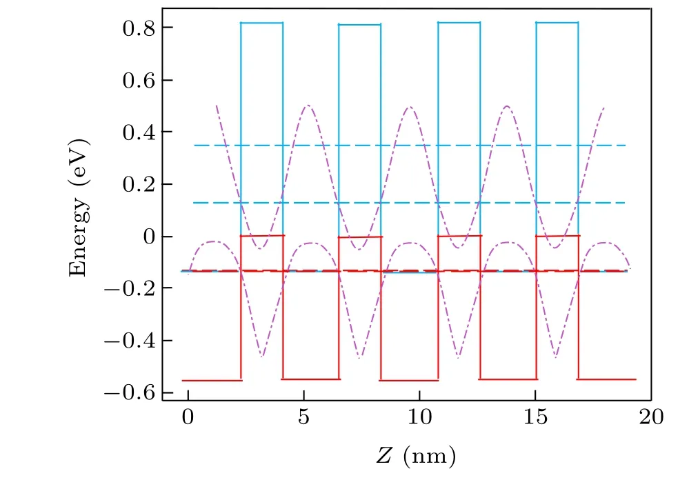
Fig.1. Band simulation results of the InAs(8 ML)/GaSb(6 ML)T2SL structure.
The samples were grown on n-type doped GaSb (100)substrates and a 500 nm GaSb buffer layer using a multichamber 3-inch wafer ultrahigh vacuum MBE system (Komponenten Octoplus 400). Firstly,the GaSb substrates were deoxidized at 520◦C for 10 min, followed by a 500 nm GaSb buffer layer grown at 460◦C with a V/III beam equivalent pressure (BEP) flux ratio value of 5.5. During the epitaxial growth, reflection high-energy electron diffraction (RHEED)was used forin-situmonitoring. When the 1×3 reconstruction pattern appears, the oxide layer has been removed. The growth temperature of the T2SLs structure was 380◦C,which was consistent with the GaSb(2×5)→(1×3)reconstructed transition temperature,and the growth rates of InAs and GaSb were 1 ˚A/s. The BEP of Sb is 2.96×10⁻⁶mbar,and the V/III BEP flux ratio value is 4 during the GaSb growth. The BEP of As is 5.74×10⁻⁶mbar,and the V/III BEP flux ratio value is 8 during the InAs growth.
The insertion of InSb between the GaSb and InAs layers of the T2SL structure has proved beneficial for strain compensation and interface quality improvement.[27]As shown in Fig. 2(a), different thicknesses (0.3 ML, 0.5 ML, 0.7 ML) of the InSb interface layer are inserted in 120 periods of InAs(8 ML)/GaSb(6 ML)T2SLs,denoted as sample A,B,and C,respectively.
The shutter sequence for the T2SL’s growth is shown in Fig.2(b). The GaSb epitaxial layers are soaked by Sb for 6 s,followed by an artificially added InSb interface layer. After InAs epitaxy, 6 s As soaking helps to prevent As from escaping from the surface and thus diffusing the surface atoms fully. The following InSb-like interfacial layers play a significant role in preventing the formation of a GaAs-like interface that adversely affects photoluminescence performance.
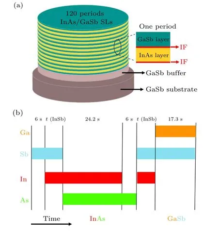
Fig.2. (a)A schematic diagram of the InAs/GaSb T2SLs multilayer heterostructure. (b)The shutter sequence for the T2SL’s growth.
3. Results and discussion
3.1. The effect of the InSb interface layer on the quality and morphology
Figure 3(a) shows the high-resolution XRD curve of the 2θ–ωscan at the GaSb (004) reflection for sample A. The sharp and distinct satellite peaks reveal excellent crystal quality. Figure 3(b)shows the XRD curves for the T2SLs with the InSb layer changing from 0.3 ML,0.5 ML,and 0.7 ML.The 0-th order peaks of the structure are on the left of the GaSb substrate peak,indicating that the T2SL’s structure is in compressive strain. The angle differences between the GaSb substrate and T2SL’s structure are 0.24◦, 0.13◦, and 0.05◦as the thickness of the InSb layer decreases. The InSb interface can effectively compensate for the compressive strain between the InAs layer and GaSb substrate to realize the structure’s strain balance control. The FWHMs of the 0-th order peaks measured in Ω mode are 33–39 arcsec,indicating the high crystal quality.
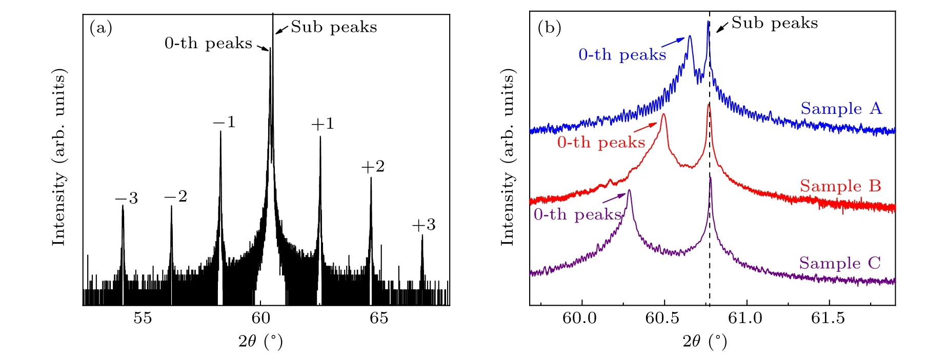
Fig.3. (a)The XRD curve of the 2θ–ω scan around the GaSb(004)reflection for sample A.(b)The XRD close-ups around the substrate and the 0-th satellite of the three samples.
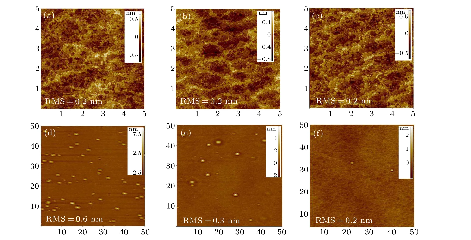
Fig.4. The morphology of a 5µm×5µm scan area using AFM for(a)sample C,(b)sample B,and(c)sample A,and a 50µm×50µm scan area for(d)sample C,(e)sample B,and(f)sample A.
The AFM morphologies are obtained on the surface of the GaSb layer. The AFM images of the three samples are shown in Fig.4, and all the samples showed minor RMS roughness.As shown in Figs. 4(a)–4(c), the samples have clear atomic steps with widths that are about 1µm. The V group elements that are more sensitive to temperature cannot diffuse well at low temperatures,leading to the discontinuous step edge. The bright spots of the uppermost GaSb layer in Fig. 4 are a frequently encountered difficulty in superlattice growth. There is no noticeable effect on crystal quality,verified by the XRD analysis in Fig.3. With the decrease in the InSb thickness,the number of bright spots is reduced,and the height decreases,indicating that the bright spots may also be related to the strain.
3.2. TEM investigations
HRTEM and high-angle annular dark-field scanning transmission electron microscopy (HAADF-STEM) were used to characterize the interface at the atomic scale. The spherical aberration electron microscope samples were prepared by focused ion beam (FIB) cutting. InAs and GaSb layers are distinguishable in Fig. 5(a), and the interfaces are smooth without any microscopic defects and dislocations.The superlattice structure of alternating growth of InAs and GaSb along the growth direction is consistent with the multilayer stack,as shown in Fig.2(a).
The color images in Fig.5(b)can intuitively observe the anion–cation dumbbells of GaSb and InAs. In and Sb atoms are visually brighter and bigger,related to their higher atomic number. The atomic integrated intensity analysis is performed on a row of atoms along the[100]growth direction,as shown in Fig.5(b). We can distinguish the InAs,GaSb,and interface layer in that the strength of the atomic column is proportional to the atomic number.[8,28]The interfacial region between the InAs and GaSb layers can be identified by the transition of the atomic integral intensity. The atomic integrated intensities of anions and cations are almost equal in the interfacial region,indicating that the InSb interface is formed, which is consistent with the shutter sequence.
Figure 5(c) shows the energy dispersive spectroscopy(EDS) mapping of sample A. In together with As and Ga together with Sb are distributed in the InAs and GaSb layers,respectively,and we can observe clear spatial separation. The ratio of group V to group III is almost 1:1 in Fig.5(d),and an apparent intensity flipping of the atomic columns can be observed in the adjacent layers. The element distribution profile of Sb atoms is comparatively wider than that of Ga atoms,indicating it is Sb-rich in the interfacial region. This also proves that the shutter sequence is effective.
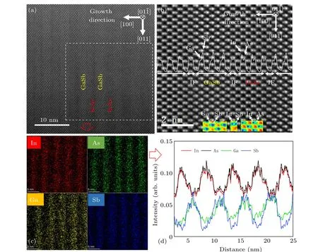
Fig. 5. (a) A HRTEM image of the InAs/GaSb multilayer structure of sample A. (b) A HAADF-STEM micrograph taken from sample A. The inset linear intensity profile along a selected row shows the InAs,GaSb,and interface layers. (c)EDS mapping of sample A.(d)Elemental integral intensity in the growth direction.
3.3. Characterization of optical properties
Figure 6(a) displays the PL spectra at 77 K for different thicknesses of the InSb interface layer. With the thickness of the InSb interface increasing, the wavelength of SL shows a redshift, and the bandgap decreases. The PL FWHM and maximum peak positions of the three samples are shown in Figs. 6(c) and 6(d). The FWHM of the PL is only 18 meV,17 meV, and 16.5 meV. The peak wavelengths are 4.78 µm(259 meV),5.02µm(247 meV),and 5.49µm(226 meV)for sample A,B,and C,respectively.The roughness and steepness of the interface affect the crystal quality,and the PL spectrum also reflects the excellent growth of the interface.
It can be seen from Fig. 6(b) that the intensity of the luminescence peaks gradually decreases with increasing temperature. According to the Fermi–Dirac distribution law,the energy distribution of the conduction electrons becomes more concentrated when the temperature drops. When photoexcitation occurs at low temperatures, excited carriers are more densely distributed in the narrow high-energy state.The luminescence peak intensity shows more intense and sharper peaks due to the concentrated photons that are produced when carriers return back to lower energy levels.[29]The luminescence peaks’ redshift corresponds to the narrow bandgap energy,consistent with the empirical relationship between bandgap energy and the photon wavelength. The linearquadratic relation proposed by Varshni can explain:[30,31]
whereEg(0) is the bandgap at zero temperature, andαandβare the intrinsic constants of the materials. Here,Eg(0)∼0.26 eV and the Debye temperatureβ ∼400 K, whileα ∼0.277 meV describes the effect of electron–phonon interaction on the energy band. The atomic vibration amplitude increases when the temperature rises,and the electron vibration interaction significantly affectsEg(T). From 77 K up to 150 K, the position of the response peaks shifts 0.15µm,and the intensity is reduced by 59%. The PL results proved that the InAs/GaSb T2SLs obey temperature-dependence properties.
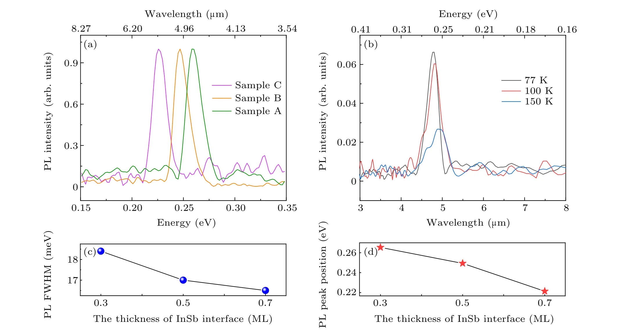
Fig. 6. (a) Normalized PL spectra at 77 K, (c) the PL FWHM and (d) the PL peak positions for different thicknesses of the InSb interface layer.(b)Variable temperature PL spectra of sample A at 77 K,100 K,and 150 K.
4. Conclusion
We have optimized the strain-balanced InAs/GaSb T2SLs of the MWIR range by designing InSb interface layers systematically. The 120 periods of InAs (8 ML)/GaSb (6 ML)T2SLs with different thicknesses of the InSb interfaces have been grown at 380◦C using MBE.The HRXRD and AFM results display excellent crystal quality and smooth morphology.The surface “bright spots” appear to be more apparent as the InSb interface thickness increases. From the HRTEM results,we can distinguish the clear interface of InAs, GaSb, and the interface layers. Using PL testing,the experiment wavelength is close to the simulated wavelength using thek·pmodel. The PL measurements also indicate that the InSb interface and the operating temperature can influence the optical properties. In conclusion,the design involving insertion of the InSb interface layer can effectively optimize the growth quality of epitaxial materials,and provides a new idea for focal plane growth.Further device-processing technology and device-level performance will be developed and demonstrated.
Acknowledgments
Project supported by the Beijing Scholars Program(Grant No.74A2111113),the Research Project of Beijing Education Committee(Grant No.KM202111232019),the National Natural Science Foundation of China(Grant No.62105039),and the Research Project of Beijing Information Science&Technology University(Grant No.2022XJJ07).
猜你喜欢
黄河之声(2022年3期)2022-06-21
黄河之声(2021年6期)2021-06-18
音乐教育与创作(2020年11期)2020-11-17
草原歌声(2020年2期)2020-09-25
学生天地(2020年3期)2020-08-25
乐府新声(2019年2期)2019-11-29
中国三峡(2016年5期)2017-01-15
中国三峡(2016年5期)2017-01-15
家庭用药(2016年9期)2016-12-03
学习月刊(2015年6期)2015-07-09

- Chinese Physics B的其它文章
- Editorial:Celebrating the 30 Wonderful Year Journey of Chinese Physics B
- Attosecond spectroscopy for filming the ultrafast movies of atoms,molecules and solids
- Advances of phononics in 20122022
- A sport and a pastime: Model design and computation in quantum many-body systems
- Molecular beam epitaxy growth of quantum devices
- Single-molecular methodologies for the physical biology of protein machines