
Laser-Induced Graphene Conductive Fabric Decorated with Copper Nanoparticles for Electromagnetic Interference Shielding Application
2023-12-28 08:47LIUWanling刘琬玲CHENChunhui陈春晖HAIWenqing海文清BISiyi毕思伊JIANGJinhua蒋金华SHAOHuiqi邵慧奇SHAOGuangwei邵光伟FUShaoju付少举CHENNanliang陈南梁
LIU Wanling(刘琬玲), CHEN Chunhui(陈春晖), HAI Wenqing(海文清), BI Siyi(毕思伊)*, JIANG Jinhua(蒋金华), SHAO Huiqi(邵慧奇), SHAO Guangwei(邵光伟), FU Shaoju(付少举), CHEN Nanliang(陈南梁)*
1 Shanghai Frontier Science Research Center for Modern Textiles, College of Textiles, Donghua University, Shanghai 201620, China
2 Engineering Research Center of Technical Textiles, Ministry of Education, Donghua University, Shanghai 201620, China
Abstract:To meet the demands for flexible electromagnetic interference(EMI) shielding materials, a type of conductive fabric is prepared by generating three-dimensional(3D) porous laser-induced graphene (LIG) in situ on the surface of the aramid fabric (AF) and then electroless plating copper. After LIG treatment, the porous AF demonstrates admirable conductivity due to the generation of graphene. The superior surface resistance of the conductive fabric can reach 1.57 Ω/sq after copper deposition, and the average EMI shielding effectiveness (SE) can reach 34.3 dB in a frequency range of 8.2 to 12.4 GHz, with the EMW absorption accounting for about 80%. The proposed technology provides a new idea for preparation of flexible EMI shielding materials.
Key words:laser-induced graphene (LIG); electroless plating; aramid fabric (AF); electromagnetic interference (EMI)
0 Introduction
The emergence of the Internet and related electronic products relying on electromagnetic waves (EMWs) to transmit information over long distances has brought people into a more convenient and efficient life[1-2]. Meanwhile, electromagnetic radiation caused by excessive use of electronic equipment has aroused people’s concern[3-4]. EMW pollution not only disturbs the normal operation of instruments but also harms human tissues and organs[5-6]. Therefore, it is important to develop electromagnetic interference (EMI) shielding materials with high shielding effectiveness (SE). When EMWs act on shielding materials, the shielding response is associated with different wavelengths of EMWs which can be divided into reflection, absorption and transmission according to the action mechanism. In terms of Schelkunoff theory, the classical theory of EMI shielding, the shielding effects of shielding materials on EMWs mainly include reflection loss on the surface and the interface between different components of materials, absorption loss inside materials and multiple reflection attenuation[7-9].
At present, EMI shielding materials are mainly divided into metal materials and non-metal materials. Metals including copper, cobalt, nickel,etc. are reflected-dominant materials, and non-metal materials including carbonic materials, conductive polymers, MXenes,etc.are absorption-dominant materials[10-12]. The metal block has prominent shielding performance but is heavy, and thus does not meet the requirement of lightweight. While carbonic materials such as graphene, carbon nanotubes and graphene oxide have low density but undesirable EMI SE. As a result, the combination of carbonic materials and metals is supposed to reduce weight and achieve a high EMI SE. However, the existing methods of graphene preparation like the mechanical stripping method, the redox method, the chemical vapor deposition method and the electrochemical method are complex and inefficient, and may cause environmental pollution[13-14], which are common problems to be solved.
In 2014, Linetal.[15]first irradiated the surface of a commercial polyimide film with a CO2laser. The high temperature generated by the CO2laser led to surface carbonization of the polymer, and other components were released in the form of gas, thus producing three-dimensional (3D) porous laser-induced graphene (LIG). Wangetal.[16]proved that no catalyst was needed in LIG preparation, and the quality of LIG was only related to laser power. There are also many researches on flexible sensors and filtration materials of LIG[17-20]. In terms of EMI shielding, Li[21]used the laser to prepare LIG on a polyether-ether-ketone (PEEK) plate and carbon fiber/PEEK (CF/PEEK) composite, which significantly improved the EMI shielding performance of the material. Yuetal.[22]used polybenzoxazine as the precursor to prepare LIG and then used a solvent-free method to prepare LIG/Fe3O4composite, achieving both lightweight and admirable EMI shielding performance. Yinetal.[23]prepared 3D LIG on a polyimide substrate, and then modified nickel nanoparticles (NPs) in the LIG network to make thin films. The SE of the prepared sample is better than that of most carbon-based and nickel-based EMI shielding materials. Hence, laser induction is an economical, convenient and green method for graphene preparation. In addition, the generated 3D porous structure is beneficial to SE improvement[24].
As mentioned above, the metal block is heavy, while the metallic film is an alternative with the advantage of being lightweight. The thin metallic film is easily adhered to various conductive and insulated substrates like metal, paper, textiles, wood,etc.through magnetron sputtering, electroless plating, vapor deposition, electroplating,etc.[25-29], among which electroless plating is widely used due to its advantages such as uniform coating, strong adhesion and easy operation. Consequently, electroless plating on LIG is considered as an effective strategy to generate a synergistic effect on the enhancement of SE.
In this work, the surface of the aramid fabric (AF) is treated by the laser to generate 3D porous graphene. The influences of the laser power and the filling spacing on the quality of graphene are explored and the corresponding microstructures are characterized by scanning electron microscopy (SEM) and Raman spectroscopy. Electroless copper plating is performed to enhance the conductivity and EMI shielding properties of the fabric. The influence of electroless plating time is discussed, and X-ray photoelectron spectroscopy (XPS), X-ray diffraction (XRD) and SEM characterizations are performed to demonstrate the microstructures. The prepared fabric displays a high EMI SE, which indicates a brilliant future in EMI shielding applications.
1 Experiments
1.1 Materials
The AF (aramid 1414 needled nonwoven fabric) with 288 g/m2area density, 2.8 mm thickness and 1.5 m width was purchased from Changzhou Hualike New Material Co., Ltd., China. All chemicals (analytically pure) were purchased from Sinopharm Chemical Reagent Co., Ltd., China, and used without further purification.
1.2 Sample characterization
A scanning electron microscope (SU8010, TM3000, HITACHI, Japan) was used to observe the microscopic morphology of the samples. The quality of LIG was evaluated by using a laser micro-Raman spectrometer (Via-Reflex, Renishaw, UK). A four-probe tester (ST2258C, Suzhou Jingge Electronic Co., Ltd., China) was used to measure the square resistance of the samples after laser induction and electroless plating. The square resistance was measured five times to obtain an average value. An X-ray photoelectron spectroscope (Escalab250Xi, ThermoFisher Scientific, USA) was used to test the elements and valence states of the samples. The metallic crystal structure of the electroless plating samples was analyzed by using an X-ray diffractometer (Bruker D8 ADVANCE, Bruker, Germany). A vector network analyzer (PNA-N5244A, Agilent, USA) was used to test the EMI shielding performances of the samples.
1.3 Sample preparation
1.3.1LIGgeneration
1)The AF was cut into a square with a size of 4 cm×4 cm, and ultrasonically cleaned with deionized water and ethanol for 5 min to remove impurities and oil stains on the fabric.
2)The LIG was obtained by etching on the sample using a laser engraving machine (K6 Pro, Shanghai Diaotu Industrial Co., Ltd., China). The laser power was set at 1.2, 1.8, 2.4 and 3.0 W, respectively, and the filling spacing was set at 0.05, 0.20, 0.35 and 0.50 mm.
1.3.2Synthesisofcopper-coatedcompositefabric
1)The laser-treated graphene aramid fabric (GAF) was soaked in NiSO4solution for Ni2+ions absorption. The GAF that absorbed Ni2+ions was labeled as GAF-Ni2+.
2)GAF-Ni2+was then soaked in NaBH4solution which was used as a reducing agent to reduce Ni2+ions to Ni0NPs at room temperature for 20 min. The GAF that absorbed Ni0was labeled as GAF-Ni0.
3)Copper electroless plating was conducted by immersing GAF-Ni0in the electroless plating solution composed of 5 g/L CuSO4, 0.75 g/L NiSO4, 25 g/L KNaC4H4O6, 5 g/L NaOH, 3.75 g/L Na2CO3and 1 mol/L HCHO at 40 ℃ for 10, 20, 30 and 60 min, respectively. Ultimately, the obtained samples were rinsed with deionized water and dried in an oven at 60 ℃, which were labeled as CuGAF-10, CuGAF-20, CuGAF-30 and CuGAF-60, respectively. The AF electroless-plated for 60 min(without laser-treatment) were labeled as CuAF-60.
2 Results and Discussion
2.1 LIG characterization
Microscopic images of GAF surfaces with different filling spacing values (at 3 W laser power) are shown in Fig.1. During the etching process, the laser is carved in one direction, and the spacing of the etched fringe can be changed by adjusting the filling spacing. When the filling spacing is 0.05 mm (Fig.1(a)), there is no obvious fringe on the fabric surface, and the spacing between the lines cannot be seen under the microscope. With the increase of the filling spacing, the fringe appears on the fabric surface and the spacing between the fringes gradually increases, and the generated LIG is less, which is consistent with the operation mode of the laser during etching(Figs.1(b)-1(d)).

Fig.1 Electronic microscope images of GAF samples with different filling spacing values: (a) 0.05 mm; (b) 0.20 mm; (c) 0.35 mm; (d) 0.50 mm
The pristine AF (Fig.2(a)) shows a smooth surface. The fibers on the surface of AF were carbonized by laser treatment and accompanied by the release of gaseous products, developing a 3D porous structure. As shown in Figs.2(b)-2(e), the degree of fiber breakage on the fabric surface increases, and more cavities are generated with the increase of laser power. More heat is accumulated due to stronger laser power, which leads to greater fiber destruction on the surface and a better degree of carbonization. Thus superior quality of LIG and a 3D porous structure are generated.

Fig.2 SEM images of samples: (a) AF; (b)-(e): GAF samples obtained at the laser power of 1.2, 1.8, 2.4 and 3.0 W, respectively


Fig.3 Raman spectra of samples: (a) AF; (b) GAF samples obtained at different laser power values
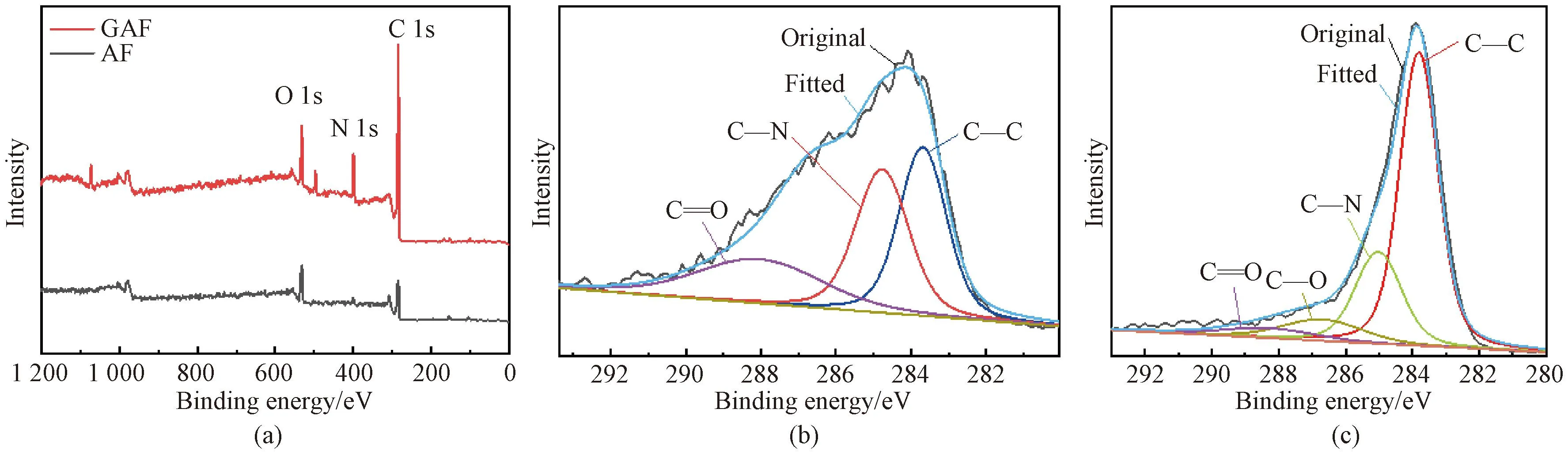
Fig.4 XPS spectra of samples: (a) wide-scan spectra of AF and GAF; (b) C 1s core-level spectra of AF; (c) C 1s core-level spectra of GAF
Figure 5 shows the changes in surface resistance of the GAF samples after laser treatment. When the filling spacing increases, the square resistance of the GAF sample increases from 0.15 kΩ/sq to 2.60 kΩ/sq (Fig.5(a)). This is because the distance between each conductive graphene line increases with the increase of filling spacing, which results in more discontinuous conductive paths. The laser power is another significant factor for conductivity, and the higher laser power leads to better carbonization quality. Figure 5(b) shows that the minimum square resistance (0.15 kΩ/sq) of the GAF sample is achieved under the conditions of 3.0 W laser power and 0.05 mm filling spacing.
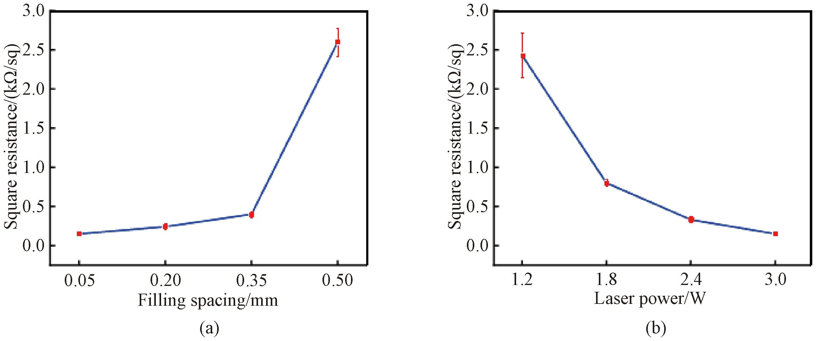
Fig.5 Relationship between square resistance and different parameters: (a) filling spacing; (b) laser power
2.2 Electroless plating characterization
The GAF samples were treated with NiSO4solution and then reduced by NaBH4before electroless plating. The SEM images of the samples before and after reduction are shown in Figs. 6(a) and 6(b). Before reduction, the fibers of GAF-Ni2+(Fig.6(a)) maintain the appearance of holes on the surface after laser treatment, and nickel sulfate can be seen uniformly attached to the fiber surface. After reduction, catalytic sites appear obviously on the fiber surface of GAF-Ni0and the distribution of catalytic sites is uniform. These catalytic sites promote the chemical deposition of metals, which is conducive to the density of the coating. Fabric samples with different plating time (CuGAF-10, CuGAF-20, CuGAF-30 and CuGAF-60) are selected to analyze micro-morphologies as shown in Figs. 6(c)-6(e). When the electroless plating time is 10 min (Fig.6(c)), some grains initially appear on the surface of CuGAF-10, and the grains are discontinuous. With the increase of electroless plating time, the grains become bigger, and the surface is gradually covered by the metal layer. After 60 min plating (Fig.6(f)), it is obvious that a dense metal coating is formed on the surface of CuGAF-60. Metal particles areinsitugrown at the dispersed and uniform catalytic sites on the graphene surface, and finally, a continuous and dense coating is formed.

Fig.6 SEM images of samples: (a) GAF-Ni2+; (b) GAF-Ni0; (c) CuGAF-10; (d) CuGAF-20; (e) CuGAF-30; (f) CuGAF-60
The surface elements and their states of the fabric samples before electroless plating were studied by XPS. The corresponding XPS spectra are demonstrated in Fig.7(a). The Ni 2p signal at about 857.0 eV[31]is observed in the spectra of GAF-Ni2+and GAF-Ni0. High-resolution Ni 2p XPS spectra are further analyzed in Figs. 7(b) and 7(c).
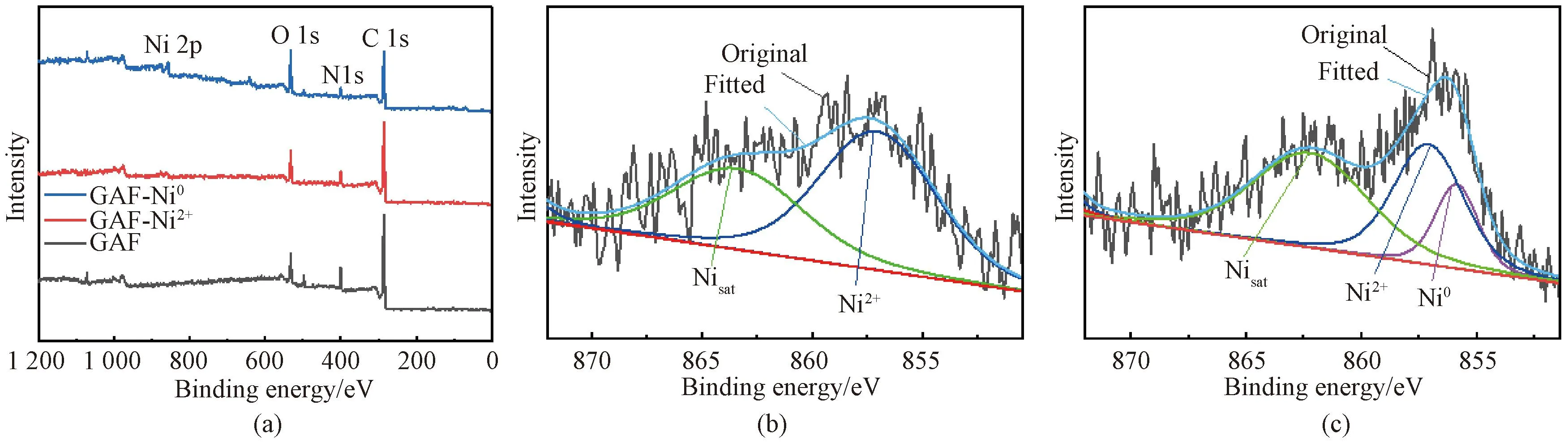
Fig.7 XPS spectra of samples: (a) full spectra; (b) Ni 2p core-level spectra of GAF-Ni2+; (c) Ni 2p core-level spectra of GAF-Ni0

Fig.8 XRD patterns of samples with different plating time
For GAF-Ni2+(Fig.7 (b)), the Ni 2p signal can be decomposed into Ni2+peak and the satellite peak of Ni (Nisatpeak) at 857.2 eV and 863.7 eV[31], respectively. As shown in Fig.7(c), afterinsitureduction with NaBH4, a new Ni0peak appears at 855.9 eV but Ni2+peak still exists, indicating that some Ni2+ions are reduced to Ni0NPs. It can be seen from the above analysis that Ni0NPs formed on the fabric surface are not only the activator of electroless plating but also the anchor point of metallic coating.
Figure 8 shows XRD patterns of samples with different electroless plating time (10, 20, 30 and 60 min). Bragg reflections at 2θof 43.3°, 50.5° and 74.2° are indexed to Cu (111), Cu (200) and Cu (220) of the hexagonal close-packed (HCP) phase according to the powder diffraction profile (PDF#01-070-3039). The characteristic lattice parameters of Cu meeta=b=c=0.361 3 nm. According to Scherrer’s formula, the mean crystalline sizedis expressed as
d=kλ/(Bcosθ),
(1)
wherekis the Scherrer constant (0.89);λis the wavelength of Cu Kα(0.154 nm);Bis the full width at half maximum (FWHM) at 2θ;θis the Bragg angle.
The calculated grain sizes of Cu NPs are 0.7, 1.0, 15.0 and 23.0 nm corresponding to the plating time of 10, 20, 30 and 60 min, respectively. With the increase of electroless plating time, Cu NPs deposit on the fabric surface and their grain sizes increase gradually.
The square resistance of samples with different electroless plating time (10, 20, 30 and 60 min) is measured as shown in Fig.9. It can be observed that the surface resistance values of the samples significantly decrease from 12.36 Ω/sq to 2.59 Ω/sq when the electroless copper plating time increases from 10 min to 60 min.
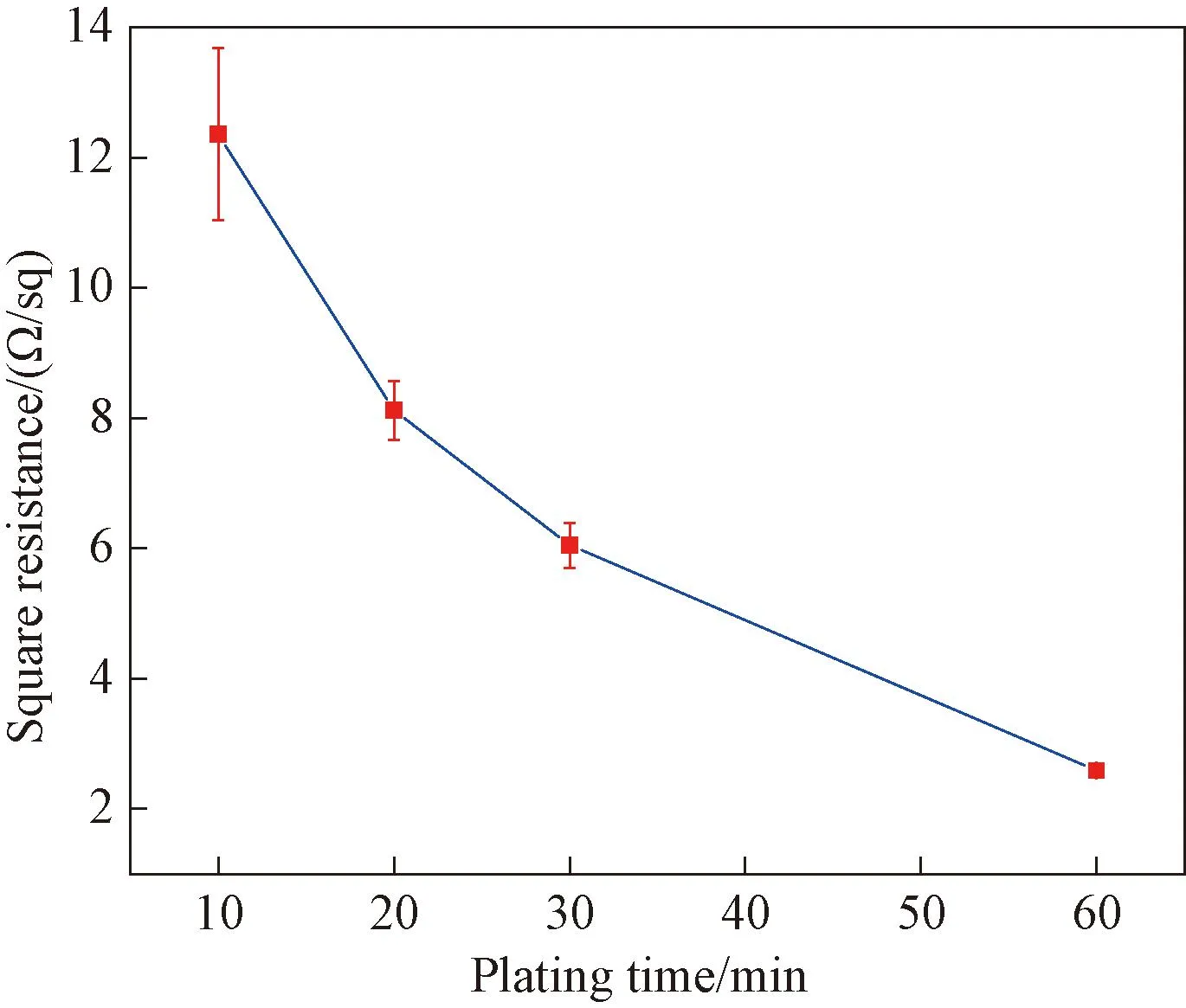
Fig.9 Square resistance of samples with different plating time
2.3 EMI shielding performance
EMI SE can be expressed as the sum of reflection loss (SE-R), absorption loss (SE-A) and internal multiple reflection loss (SE-M) of incident EMWs. When EMI SE exceeds 15 dB, the contribution of the SE-M is small and negligible[32]. The SE-R is due to an impedance mismatch between air and shielding material. A high conductive barrier shows a large impedance mismatch at the interface, resulting in the reflection loss of incident EMWs. The SE-A is the result of dielectric loss and magnetic loss.
As shown in Fig.10, SE, SE-R and SE-A values of CuGAF samples are higher than those of CuAF-60 and GAF samples in X-band (frequency range: 8.2-12.4 GHz). This is because 3D porous LIG with low conductivity has certain EMI shielding properties. After electroless plating, a metallic layer is deposited on the surface of GAF, and the metal grain can also be attached to the inside of the pores of the damaged fibers. When the incident EMWs are transmitted to the CuGAF surface, the good conductivity of the CuGAF surface causes impedance mismatch, and part of the EMWs are reflected into free space[33]. The incident EMWs are further attenuated and absorbed thanks to the multiple reflections caused by the porous structure and the interface polarization caused by the defects on CuGAF. With the increase of electroless plating time, more Cu NPs are deposited on the fabric surface and in fiber pores, and the shielding effect becomes better.
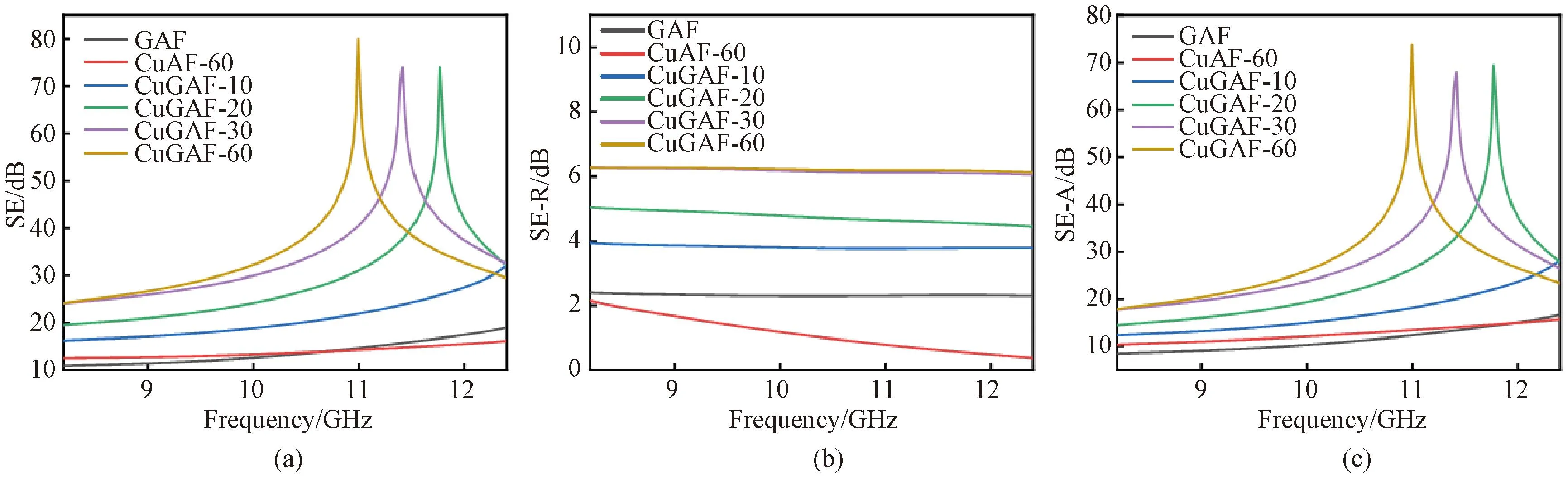
Fig.10 EMI shielding performance of samples: (a) SE; (b) SE-R; (c) SE-A
As shown in Figs. 10 (a) and 10(c), the SE peaks and SE-A peaks are obvious when the electroless plating time is 20, 30 and 60 min, which may be caused by pores between the etched fibers and several parallel planes formed between the pores. EMWs can be reflected repeatedly between two parallel planes to produce multiple coherent reflected waves. When the reflected waves are in the same phase, phase interference is developed. The improvement of SE level is due to the occurrence of phase-length interference caused by the in-phase reflection of EMWs. When electroless plating time increases, the thickness of the shielding layer does not match the distance of phase-length interference. Moreover, due to the parallel resonance absorption and phase-length interference of parallel planes, the absorption peaks of CuGAF are sharp, and the EMI SE values of CuGAF samples are desirable at specific frequencies[34].
In theory, higher conductivity leads to more reflection loss, resulting in an enhanced EMI SE value. Figure 10 (b) shows SE-R changes in various CuGAF samples. In Fig.10 (b), the curve of the sample treated only by electroless plating (CuAF-60) shows a downward trend with increasing frequency due to the impedance matching between air and the sample.
When the electroless plating time reaches 60 min, the average SE and SE-A of CuGAF-60 are 34.3 and 28.1 dB respectively in X-band. The calculated absorption ratio (SE-A/SE) is 81.9%, and the shielding efficiency[35]is 99.9%. In addition, it is worth noting that the highest SE value of CuGAF-60 is about 80 dB at 10.9 GHz. The EMI SE values of CuGAF-60 and other shielding materials[36-38]are summarized in Table 1 and it can be seen that CuGAF-60 prepared in this work demonstrates relatively high EMI SE value in X-band.
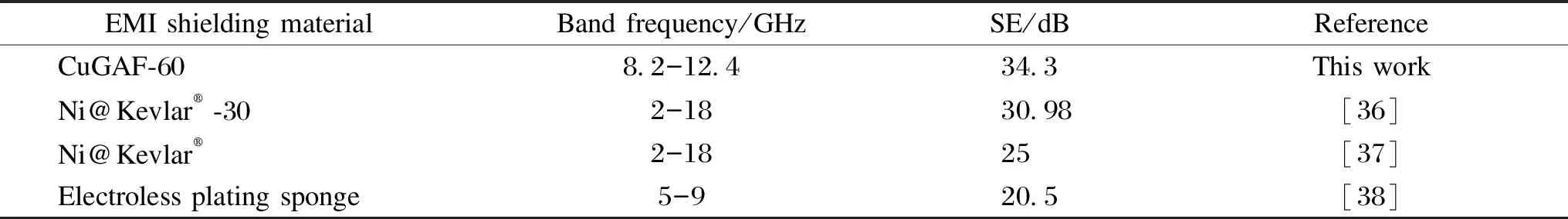
Table 1 EMI SE values of CuGAF-60 sample and other shielding materials
3 Conclusions
In this study, the LIG is generated on the surface of the AF by laser etching, which is confirmed by Raman and XPS characterization. A cost-effective electroless plating method is then used to obtain the superior conductive Cu coating on GAF. The optimal laser parameters (the laser power is 3.0 W, and the filling spacing is 0.05 mm) are determined by square resistance measurements to obtain a better conductivity (1.57 Ω/sq). By using SEM, XPS and XRD, it is confirmed that with the extension of electroless plating time, more Cu NPs are deposited on the surface of GAF, thus forming a dense coating. EMI SE values of CuGAF samples with different electroless plating time are tested. As a result, the EMI SE of CuGAF-60 can reach 34.3 dB in X-band, and its absorption accounts for 81.9%. The proposed technology provides a new idea for the processing and manufacturing of EMI shielding materials.
猜你喜欢
当代作家(2023年5期)2023-07-10
大江南北(2022年11期)2022-11-08
中老年保健(2022年2期)2022-08-24
鸭绿江(2021年17期)2021-11-11
宝藏(2021年1期)2021-03-10
收藏家(2021年10期)2021-01-17
新世纪智能(语文备考)(2019年12期)2020-01-13
阅读(快乐英语高年级)(2019年2期)2019-09-10
Chinese Physics B(2019年7期)2019-08-06
陶瓷科学与艺术(2018年1期)2018-07-13
 Journal of Donghua University(English Edition)2023年6期
- Journal of Donghua University(English Edition)的其它文章
- Toughness Effect of Graphene Oxide-Nano Silica on Thermal-Mechanical Performance of Epoxy Resin
- Photoactive Naphthalene Diimide Functionalized Titanium-Oxo Clusters with High Photoelectrochemical Responses
- Preparation and Thermo-Responsive Properties of Poly(Oligo(Ethylene Glycol) Methacrylate) Copolymers with Hydroxy-Terminated Side Chain
- Synthesis, Characterization and Water Absorption Analysis of Highly Hygroscopic Bio-based Co-polyamides 56/66
- Design of Online Vision Detection System for Stator Winding Coil
- Clothing Parsing Based on Multi-Scale Fusion and Improved Self-Attention Mechanism