
ZnO whiskers growth on the surface of Sn9Zn/Cu solder joints in concentrator silicon solar cells solder layer①
2017-09-25 12:53ZhangLiangYangFanZhongSujuan
High Technology Letters 2017年3期
Zhang Liang (张 亮), Yang Fan, Zhong Sujuan
(*School of Mechanical & Electrical Engineering, Jiangsu Normal University, Xuzhou 221116, P.R.China)(**State Key Laboratory of Advanced Brazing Filler Metals & Technology, Zhengzhou Research Institute of Mechanical Engineering, Zhengzhou 450001, P.R.China)
ZnO whiskers growth on the surface of Sn9Zn/Cu solder joints in concentrator silicon solar cells solder layer①
Zhang Liang (张 亮)②*, Yang Fan*, Zhong Sujuan**
(*School of Mechanical & Electrical Engineering, Jiangsu Normal University, Xuzhou 221116, P.R.China)(**State Key Laboratory of Advanced Brazing Filler Metals & Technology, Zhengzhou Research Institute of Mechanical Engineering, Zhengzhou 450001, P.R.China)
ZnO whiskers observation on the surface of SnZn/Cu solder joints in concentrator silicon solar cells solder layer is reported. In the experiment, SnZn/Cu samples are left in laboratory after reflow soldering for two years before an examination by SEM, then ZnO whiskers can be observed obviously, which grows out from the rich-Zn phase of the samples and causes electrical short circuit in the electronics appliances, which demonstrates that the SnZn solder shows a risk for the short circuiting failure of an electronic device. Moreover, the growth mechanism of ZnO whiskers is researched based on cracked oxide theory, which provides the reference support for SnZn solders application.
ZnO whiskers, reflow soldering, short circuiting failure, electronic device
0 Introduction
Concentrator silicon solar cells manufactured are soldered to a metal core printed circuit board, especially for the Cu substrate, and the solder layer of the concentrator silicon solar cells will affect the reliability of the whole structure[1]. Because lead is toxic, hazardous to human health, and not friendly to environment, electronic industries are striving to find viable alternatives to tin-lead (SnPb) solders in order to meet world-wide regulatory requirements on the restrictions of the use of lead (Pb)[2,3]. Due to environmental and health concerns, extensive investigations have been made over the last few years to find an acceptable lead-free solder for various electronic attachment applications and optoelectronics modules[4]. Sn9Zn solder alloy was proposed as a low melting alternative to SnPb solders because the former’s melting point (198℃) is close to that of the latter (183℃)[5]. Therefore, eutectic Sn9Zn solder can be extensively used as interconnection, especially for solder layer of concentrator silicon solar cells.
Sn9Zn alloys were utilized in 3D packaging interconnection with SnZn/Cu and Cu/SnZn/Cu nanoscale thickness by Li[6], and the solder layer was totally consumed in the reflow process, and only Cu6Sn5and Cu3Sn phases were observed clearly at the interface. Zhang[7]demonstrated that the fatigue life of Sn9Zn solder joints in CSP device was higher than SnPb, SnAg and SnSb solder joints, and lower than that of SnAgCu solder joints. Sn9Zn solder joints represent excellent properties in electronic packaging, however, the low corrosion resistance is considered as the main issue for SnZn solder joints, because corrosion reduces solder joint strength for the formation of pits and corrosion products[8,9]. Up to now, no literature reports that Sn9Zn alloy shows a risk for electronic interconnection.
In this work, the Sn9Zn/Cu samples soldered with reflow soldering, have been stored for two years in the laboratory with ambient environment, and then were investigated again, to analyze the microstructure evolution of solder joints. The ZnO whiskers were found on the surface of Sn9Zn/Cu surface, which is the first time to report this phenomenon in lead-free solder joints.
1 Experiment
Commercial Sn9Zn paste was put on the surface of Cu substrate, and interconnection between Cu and SnZn paste was carried out by reflow soldering with peak temperature 230℃. The samples were saved for two years in the laboratory atmosphere, then cut and the cross-section was treated, the microstructures of SnZn/Cu solder joint were characterized using a solution of 5% (vol.) HNO3and 95%CH3OH for 7s. Then the phases in the matrix microstructure were determined after seven days aging under room ambience scanning electron microscope (Quanta200) equipped with a thermo-electron x-ray energy dispersion spectrometry (EDS).
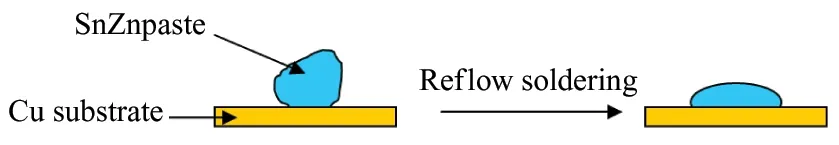
Fig.1 Schematic illustration of Sn9Zn solder joint
2 Results and discussion
The Sn9Zn eutectic solder consists of two phases, namely, the β-Sn and rich-Zn phases, as shown in Fig.2. Accompanying the microstructures observation, it was noted that whiskers growth took place in the matrix microstructure of SnZn/Cu solder joints. Fig.3 and Fig.4 show the growth of a crystal whisker on the SnZn solder joints surface with scanning electron microscopic
images, and the mapping element analysis demonstrates that the whiskers are the Zn-O composites. Moreover the root area of whiskers are rich-Zn phases, the Zn is notable for its high chemical activity, it can react with the oxygen (2Zn+O2→2ZnO) much more easily in the air and accelerate ZnO whisker growth in SnZn/Cu solder joints. The length of ZnO whiskers in Fig.2 and Fig.3 are 35μm, 15μm respectively, and the average diameter of ZnO whisker is 5μm. Moreover, only on the surface of bulk rich-Zn phase, the ZnO whiskers can be observed, no whiskers can be found on small rich-Zn phase. This phenomenon indicates that the whisker growth is related to the sizes of rich-Zn phase.

Fig.2 Microstructure of Sn9Zn solder

Fig.3 The ZnO whisker of SnZn/Cu solder joints with needle morphology

Fig.4 The ZnO whisker of SnZn/Cu solder joints with bulk morphology
Fig.5 shows the different morphologies of ZnO whiskers, it is found that all the whiskers grow out from the dark stick-like rich-Zn phase, and needle-like and bulk-like morphologies for ZnO whiskers can be observed obviously, and the longest whisker in SnZn/Cu solder joints observed by SEM is about 38μm. Fig.6 shows the distribution of ZnO whiskers in the SnZn solder matrix, different morphologies of ZnO whiskers can be observed in this picture, the roots of ZnO whiskers are all from the rich-Zn phases. For the chip stacking in 3D packaging, the size and the distance is about 20μm and the whisker is long enough to short two neighboring micro-bumps. It is possible that when there is a high electrical field crossing the narrow gap between the tip of a whisker and the point of contact on the other micro-bumps, just before the tip of the whisker touching the other micro-bump, a spark may ignite fire[10], which can result in short circuit failure of the

Fig.5 The relationship between ZnO whisker and rich-Zn phase
device, like the short circuit failure induced by whiskers as shown in Fig.7[11]. Moreover, in the high-density device, the failure can also be found between two neighboring leads or solder joints. Tu[12]established the broken oxide model to explain the Sn whisker growth, the growth of whisker is an eruption from the oxidized surface, which has to break to form Sn whisker. For ZnO whisker growth in the research, oxidation is essential too, but the ZnO whisker formed results from the accumulation of Zn-O reaction, and the growth site is the root of the ZnO whiskers.

Fig.6 Distribution of ZnO whiskers in matrix
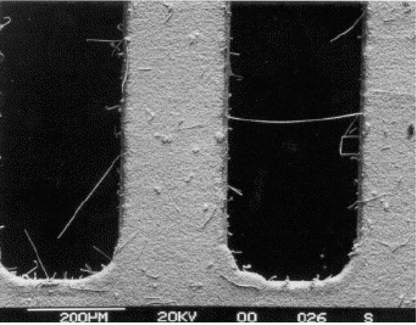
Fig.7 Short circuiting failure inducing by whiskers
In order to clarify the growth mechanism of ZnO whiskers in the SnZn/Cu solder joints in our research, the schematic illustration in Fig.8 was plotted. The bulk stick-like rich-Zn phase can precipitate from the molten SnZn solder joints, due to the touch of rich-Zn phase with oxygen, the oxidation reaction between Zn and O2may happen and the volume of rich-Zn phase will expand obviously, so the stress potential gradient can be formed while the stress is a necessary condition for spontaneous whiskers growth, so it is believed that the driving force for ZnO whisker growth is related to the stress potential gradient developed in the rich-Zn phase. Chen[13]found the stress resulting in the Sn whisker growth was tensile residual stress not compressive stress in Sn-Mn alloy electrodeposits. Ye[14]suggested that the compressive stress is the driving force for Sn whisker growth during thermal cycling. Therefore, for ZnO whiskers, the stress driving the formation of whiskers growth in SnZn/Cu solder joints should be determined further. Moreover, due to volume expanding, the neighboring Sn matrix will deform simultaneously, so the crack can be found in the Sn matrix around ZnO phase, as shown in Fig.8 and the crack phenomena can be observed in the SEM figure (see Fig.9). Meanwhile, the cracks of Sn matrix can provide the paths for the touching of oxygen with rich-Zn phase, only when the rich-Zn phase reacts with oxygen completely. All Zn in the rich-Zn phase will be squeezed into ZnO whisker, then the oxidation procedure and whiskers growth will cease. Therefore, the whiskers growth and the whiskers length are determined by the rich-Zn sizes. Fig.10 shows the effect of Zn content on the ZnO whisker growth, it is found that with the decrease of Zn, the ZnO whiskers can be reduced significantly, and no ZnO whiskers can be observed in Sn-1Zn and Sn-2Zn. Since the Zn content in SnZn solder is 9wt.%, the oxidation can be found obviously. When the content of Zn is reduced to an extent in SnZn solder (1%Zn and 2%Zn), the rich-Zn phase is too small to provide the stress potential gradient during oxidation, the ZnO whiskers may be not formed in the small rich-Zn phases for low Zn SnZn solders. So the Sn9Zn eutectic solder shows a risk for the short circuiting failure of electronic device, the application of Sn9Zn solder should be considered carefully in concentrator silicon solar cells.

Fig.8 Growth mechanism of ZnO whisker
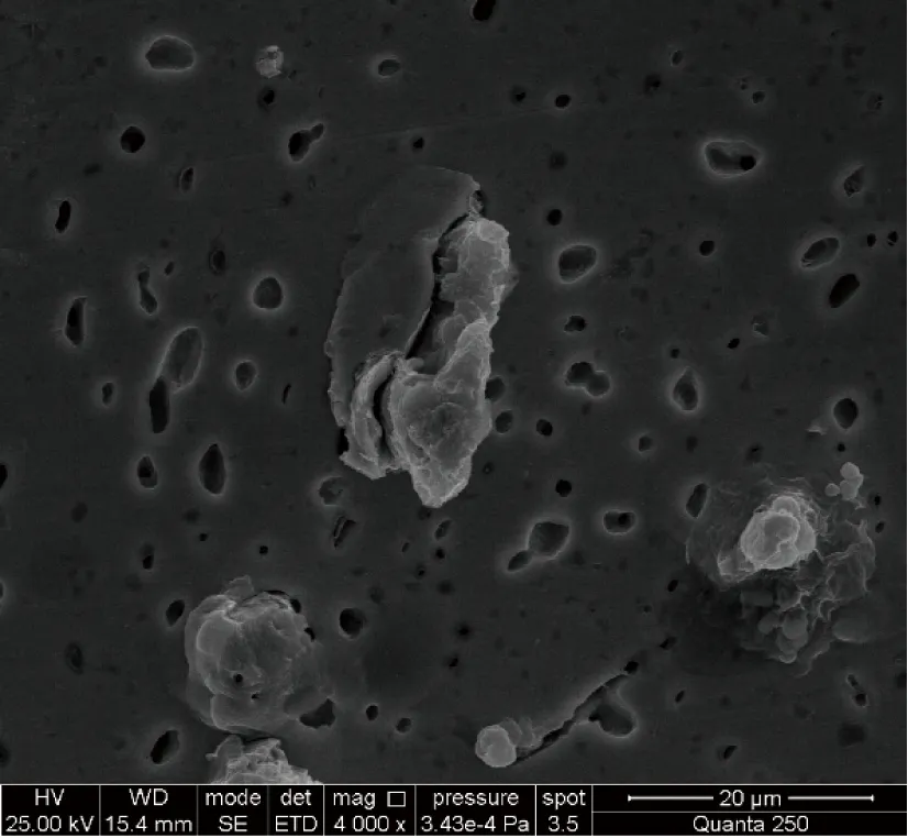
Fig.9 Crack in the matrix around ZnO whisker
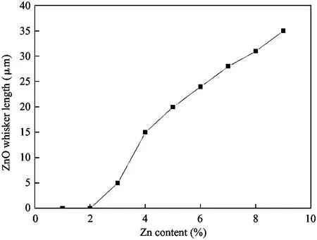
Fig.10 Effect of Zn content on the whiskers growth
3 Conclusions
ZnO whiskers in Sn9Zn/Cu solder joints of concentrator silicon solar cells solder layer are reported firstly. It is observed that the ZnO whiskers grow out from the surface of rich-Zn phase in the solder joints under room ambience. A cracked oxidation mechanism is used to explain the growth behavior of ZnO whiskers, and the whiskers may increase the risk of short circuit failure in electronic devices. Such a phenomenon of abnormal whisker growth may significantly degrade the reliability of whole assembly.
[ 1] Baricordi S, Calabrese G, Gualdi F, et al. A joint thermal-electrical analysis of void formation effects on concentrate silicon solar cells solder layer. Solar Energy Materials Solar Cells, 2013, 111(4): 133-140
[ 2] Zhang L, Han J G, Guo Y H, et al. Properties and microstructures of SnAgCu-xEu alloys for concentrator silicon solar cells solder layer. Solar Energy Materials Solar Cells, 2014, 130: 397-400
[ 3] Zhang L, Tu K N. Structure and properties of lead-free solders bearing micro and nano particles. Materials Science Engineering Reports, 2014, 82(1): 1-32
[ 4] Meydaneri F, Saatci B, Gündüz M, et al. Determination of thermal conductivities of Sn-Zn lead-free solder alloys with radial heat flow and Bridgman-type apparatus. Continuum Mechanics and Thermodynamics, 2013, 25(6): 691-704
[ 5] Shrestha T, Gollapudi S, Charit I, et al. Creep deformation behavior of Sn-Zn solder alloys. Journal of Materials Science, 2014, 49(5): 2127-2135
[ 6] Li Q Q, Chan Y C, Zhang K L, et al. Study of microstructure evolution in novel Sn-Zn/Cu bi-layer and Cu/Sn-Zn/Cu sandwich structures with nanoscale thickness for 3D packaging interconnection. Microelectronic Engineering, 2014, 122(16): 52-58
[ 7] Zhang L, Sun L, Guo Y H, et al. Reliability of lead-free solder joints in CSP device under thermal cycling. Journal of Materials Science: Materials in Electronics, 2014, 25(3): 1209-1213
[ 8] Ghaddafy M G, Yahaya M Z, Mohamad A A. Corrosion of Sn-9Zn solder joints: a review. International Journal of Electroactive Materials, 2014, 2: 8-16
[ 9] Zhang L, Han J G, Guo Y H, et al. Microstructures and properties of SnZn lead-free solder joints bearing La for electronic packaging. IEEE Transactions on Electron Devices, 2012, 59(12): 3269-3272
[10] Tu K N, Li J C M. Spontaneous whisker growth on lead-free solder finishes. Materials Science & Engineering: A, 2005, 409(1-2), 131-139
[11] Tu K N, Chen C, Wu A T. Stress analysis of spontaneous Sn whisker growth. Joural of Materials Science: Materials in Electronics, 2007, 18(1):269-281
[12] Tu K N. Electronic Thin-Film Reliability. Cambridge: Cambridge University Press, 2011
[13] Chen K M, Wilcox G D. Observations of the spontaneous growth of tin whiskers on tin-manganese alloy electrodeposits. Physical Review Letters, 2005, 94(6): 066104
[14] Ye H, Xue S B, Petcht M. Effects of thermal cycling on rare earth (Pr)-induced Sn whisker/hillock growth. Materials Letters, 2013, 98(5): 78-81
Zhang Liang, born in 1984. He is currently a professor in School of Mechatronic Engineering, Jiangsu Normal University, China. He received his Ph.D degree from Nanjing University of Aeronautics and Astronautics, China in 2011. His research interests include microelectronics welding, SMT, lead-free solders. etc. He has published over 100 papers.
10.3772/j.issn.1006-6748.2017.03.016
Supported by the National Natural Science Foundation of China (No. 51475220), the State Foundation of Laboratory of Advanced Brazing Filler Metals & Technology (Zhengzhou Research Institute of Mechanical Engineering) (No. SKLABFMT-2015-03) and High Level Talent Plan of Jiangsu Normal University (No. YQ2015002).
To whom correspondence should be addressed. E-mail: zhangliang@jsnu.edu.cn
on July 27, 2016
 High Technology Letters2017年3期
- High Technology Letters的其它文章
- Quantitative analysis of the performance of vector tracking algorithms①
- Simulation and experimental research of digital valve control servo system based on CMAC-PID control method①
- Application of linear active disturbance rejection control for photoelectric tracking system①
- Structure design of gradient hard coatings on YG8 and their residual stress analysis by ANSYS①
- Characterizing big data analytics workloads on POWER8 SMT processors①
- A leveling mechanism for the platform based on booms-constraint control of aerial vehicle①