
Electrical transport and optical properties of Cd3As2 thin films∗
2019-11-06 00:46YunKunYang杨运坤FaXianXiu修发贤FengQiuWang王枫秋JunWang王军andYiShi施毅
Chinese Physics B 2019年10期
关键词:王军
Yun-Kun Yang(杨运坤),Fa-Xian Xiu(修发贤),Feng-Qiu Wang(王枫秋),Jun Wang(王军),and Yi Shi(施毅),6,†
1Collaborative Innovation Center of Advanced Microstructures,Nanjing 210093,China
2State Key Laboratory of Surface Physics and Department of Physics,Fudan University,Shanghai 200433,China
3School of Electronic Science and Engineering,Nanjing University,Nanjing 210093,China
4School of Optoelectronic Science and Engineering,University of Electronic Science and Technology of China,Chengdu 610054,China
5State Key Laboratory of Electronic Thin Films and Integrated Devices,University of Electronic Science and Technology of China,Chengdu 610054,China
6National Laboratory of Solid State Microstructures,School of Physics,Nanjing University,Nanjing 210093,China
Keywords:topological Dirac semimetals,thin films,photodetectors,ultra-fast optical switches
1.Introduction
In remembrance of the renowned Chinese physicist Professor Kun Huang,who made significant contributions to the development of solid-state physics,we start with a brief introduction of his pioneering achievement. Huang’s research was mainly involved with many aspects of phonon physics in solids. He is widely known for his collaboration with Max Born in writing the classic monograph—Dynamical Theory of Crystal Lattices.His contributions include the concept of polaritons,Huang scattering of x-ray,the Huang–Rys factor used for describing electron–phonon interaction,and the Huang–Zhu model used for calculating electron–longitudinal phonon interaction in quantum wells and superlattices.[1–8]In recent years,Huang’s research has been widely used to study various physical problems related to low-dimensional semiconductor materials and phonons,including transport phenomena,Raman scattering,phonon polaritons,and many other frontier problems.[9–11]
While the theoretical development of phonon dynamics has tremendously benefited the academia and semiconductor industries,the novel concept of topological matters was proposed and specific material systems were discovered in recent years.One representative example of topological systems is the topological insulator(TI),which features bulk states that have an energy bandgap and gapless surface states,allowing surface carriers to have zero effective mass.[12,13]Another intriguing example is topological Dirac semimetals(TDSs).They are a new kind of Dirac material that exhibits linear energy dispersion in the bulk and can be viewed as 3D graphene.It has been proposed that TDSs can be driven to other exotic phases like Weyl semimetals and topological insulators by breaking certain symmetries.One of the most exotic physical properties of these new materials is the chirality of electrons,where the spins of electrons are in parallel or antiparallel to the direction of their motion and thus develop the righthanded or left-handed chiral electrons(widely conceived as chiral anomaly).Theories also predict that topological Dirac semimetals can be driven into a quantum spin Hall insulator with a sizeable bandgap by reducing dimensionality.Driven by these exotic physical properties,extensive experiments on angle-resolved photoemission spectroscopy,[14–17]and scanning tunneling microscopy[18]were carried out to identify the 3D Dirac fermions in these materials.
The intriguing physics of these TDSs has motivated a surge of research activities towards the development of largescale single-crystalline films for potential applications in electronics and optics. The Cd3As2is considered to be an excellent 3D TDS due to its chemical stability in air, and it also possesses novel transport phenomena such as ultrahigh mobility,[19]large magnetoresistance(MR),[20]nontrivial π Berry’s phase of Dirac fermions,[21]and chiral anomaly induced negative MR.[22,23]Previously, Cd3As2bulk materials,amorphous films,[24]nanowires,[25]and platelets[26]were prepared by various growth methods, and most of magneto-transport measurements so far have focused on Cd3As2bulk materials. However,few efforts were devoted to thin films[27–29]and nanostructures,[25,30]which may exhibit surface phase-coherent transport and quantum size limit effect,[31–33]leading to Aharonov–Bohm oscillations[34]and quantum Hall insulator states.[35]Importantly,a theoreticallypredicted TI phase and thickness-dependent quantum oscillations may also eventually emerge when the dimensionality of the system is reduced.[35,36]Therefore,it is highly desirable to fabricate superb crystallinity Cd3As2thin films for the transport study,and to develop the possible optoelectronic applications by using the Cd3As2thin film system.Here we present a brief review of our recent progress in making such ultra-high mobility Cd3As2thin films via the post-annealing process and in making heterojunction photodetectors and ultrafast optical switches.[37–40]
2.Electrical transport study in intrinsic Cd3As2 thin films
A series of wafer-scale Cd3As2thin films were grown via a molecular beam ppitaxy(MBE)system at a base pressure lower than 2×10⁻¹⁰mbar(1 bar=105Pa). Singlepolished sapphire and clean cleaved mica substrates were selected for electrical transport measurements.Before growing the Cd3As2layer,the substrates were degassed at 400◦C for 30 min to remove gas molecules absorbed on the surface.Especially,a buffer layer of CdTe was deposited on the substrates in order to achieve a better crystalline match. The Cd3As2thin film deposition was carried out on the top of the buffer layer with high-purity Cd3As2(99.999%)from dualfilament and valve-cracker effusion cells.The growth process and film thickness awere in situ monitored by the reflection high-energy electron diffraction(RHEED).
3.Results

Fig.1.(a)Schematic diagram of standard six-probe Hall bar fabricated on Cd3As2 thin films with mica substrate,used for transport measurements in the PPMS system. Crystal orientation is(112),which is perpendicular to the magnetic field(up to 9 T).(b)Zero-field temperature-dependent longitudinal resistance Rxx curves for five Cd3As2 thin films with different thicknesses ranging from 50 nm to 900 nm;Rxx drops with sample thickness reducing,indicating a thickness-induced insulator-to-metal transition.(c)Variations of carrier mobilityµwith temperature.Carrier mobility is about 3750 cm2·V−1·s−1–9750 cm2·V−1·s−1 at 2 K.(d)Sketch of band structure with band gap opening for Cd3As2 thin films.(e)MR ratio at 2 K,showing non-saturation behavior and the largest ratio reaching 343.5%.(f)Nearly linear relationship between MR and electron mobility,which drops from 343.5%to 58.8%.Figure 1 is adapted from Ref.[38].
As displayed in Fig.1(a),a standard six-probe Hall bar geometry is patterned on the Cd3As2thin film with a channel size of 1.5 mm×1 mm.Low-temperature electrical transport measurements are carried out for samples with filme different thickness in a physical properties measuring system(PPMS,up to 9 T).The zero-field resistance–temperature(R–T)curves of longitudinal magnetoresistance Rxxof the Cd3As2thin films with different thicknesses are shown in Fig.1(b)(Σ1–Σ5).Meanwhile,the transverse resistance(Rxy)versus magnetic field B is measured at T=2 K,where the negative slope of Rxyshows that electrons are the dominant charge carriers in intrinsic Cd3As2thin films.As shown in Fig.1(c),derived from the Rxy–B linear parts,the typical temperature-dependence of Hall mobility(µ)is in a range of 3.8×103cm2·V−1·s−1–9.1×103cm2·V−1·s−1at 2 K.The mobility significantly increases as the temperature T drops,which can be attributed to the alleviated electron–phonon scattering at low temperatures.Besides,the sheet carrier density(ns)at 2 K changes from 3.4×1012cm−2to 24×1012cm−2,and the corresponding carrier concentration(n3D)is determined to be 1×1017cm−3–8×1017cm−3.Figure 1(d)shows a band schematic structure for a typical Cd3As2thin film. When the dimensionality is reduced,a gap is expected to open.The Fermi levels marked in the diagrams are calculated from Shubnikov–de Haas(SdH)quantum oscillations,which will be discussed below.Comparing with the Rxx–T curves mentioned above,the relative position between Fermi levels and band edges is almost consistent with each other. Moreover,figure 1(e)exhibits that a large positive magnetoresistance(MR)at 2 K in a series of Cd3As2films shows a parabolic behavior at low fields and quasi-linear property at high fieldsIt does not show a saturated tendency when the magnetic field increases,and the maximum MR ratio is close to 343.5%at B=9 T.Especially,related to the electron mobility,the corresponding MR ratio at 9 T drops from 343.5%to 58.8%. As shown in Fig.1(f),there exists an almost linear relationship between the MR ratio and mobility,which is consistent with the previous study.[41]Due to the Dirac band structure and the high mobility in Cd3As2thin films,there are strong SdH quantum oscillations in Rxxfor most of our samples at 2 K as shown in Fig.1(e).
3.1.Post-annealing effect on intrinsic and Zn-dopedthin films
In order to further enhance the crystalline quality,the asgrown films were annealed at elevated temperatures after depositing a 120-nm-thick Al2O3capping layer on the top.It can protect the underlying thin films from being oxidized in the annealing process.Figure 2(a)illustrates the structure of the multi-layered film.Figure 2(b)shows the XRD spectra which are enlarged to highlight the change of the Cd3As2(224)peaks marked by the grey dashed line.The broader peak at the left of the(224)peak comes from CdTe(111).It is evident that(224)peaks become sharper as the annealing temperature increases.In Fig.2(c)summarized is the variation of the full width at half maximum(FWHM),which indicates that the Cd3As2film undergoes recrystallization after annealing procedure that effectively reduces the FWHM.

Fig.2.(a)Schematic illustration of capping and annealing film structure,(b)XRD patterns at different annealing temperatures,(c)value of FWHM varying with annealing temperature.Experimental data denoted as 0 ◦C in panels(b)and(c)represent the results for samples before annealing but after ALD process;and origin and OG in panels(b)and(c),respectively,represent samples before the ALD process.
The post-annealing process brings about a significant enhancement of quantum oscillations. Figures 3(a)and 3(b)show the normalized resistance changes with temperature at different annealing temperatures.Below 650◦C,the samples show a metallic behavior with a small upturn at low temperatures. In a temperature range of 0◦C–550◦C,the residue resistance ratio(RRR)decreases with the increase of annealing temperature. Once the temperature reaches 650◦C,the film shows a semiconducting behavior.
The small upturn in the R–T curves at low temperatures could have two origins.One is electron–electron interaction,and the other is weak localization. Both of the two mechanisms will lead to a very similar upturn feature in the R–T curve,i.e.,the R–T curve will be linear in the logarithmic scale at low temperatures. We examine the linear behaviors of several samples and suggest that the contribution from localization is the main contribution to the metallic-insulating transition.We then study the MRs of these samples at 2 K.As shown in Figs.3(c)and 3(d),the sample without and with annealing(at 200◦C)shows a negative MR accompanied by SdH oscillations.By further increasing the annealing temperature,the negative MR decreases but the oscillation amplitude is unchanged. When the annealing temperature exceeds 400◦C,the amplitude of oscillation is dramatically enlarged.

Fig.3.(a)and(b)R–T curves with different annealing temperatures,showing that RRR decreases with annealing temperature increasing when T<550 ◦C,tendency is opposite above 550 ◦C,and a semiconducting property occurs at higher annealing temperatures;(c)and(d)curves of oscillation amplitudes versus field,indicating that amplitude increases with annealing temperature rising.
Further,Zn is doped into Cd3As2to reduce the Fermi level.The size of Fermi surface can be extracted from the SdH oscillations.With the Zn concentration increasing,the oscillation frequency(SF)decreases and the Fermi level decreases as summarized in Table 1.For the samples with low Zn concentration,it is easier to reach a quantum limit at high magnetic fields.

Table 1.Fermi level decreasing with Zn concentration increasing.
In short,the rapid annealing process can enhance the crystal quality by reducing defects via developing a recrystallization process.After annealing,the mobility of thin films rises,while the SdH oscillations become strikingly stronger.
3.2.Cd3As2 heterojunction photodetectors
Based on the high-quality Cd3As2thin films, a Cd3As2/pentacene heterojunction photodetector is fabricated as shown in Fig.4(a).The diagram of Cd3As2/pentacene heterojunction is described in Fig.4(b). A positively-charged empty state exists in the depletion region in n-type Cd3As2,when electrons move from the n-type Cd3As2into the lower energy states of the p-type pentacene. The band is bent up near the heterojunction to form a built-in field.Pentacene,as a kind of organic matter,is chosen as the p-type material in heterojunction photodetector.The organics is accessible and low-cost so that they are hopeful to be applied to large-scale devices.Besides,the dark current of organics is low,which is important for photodetectors.
For heterojunction-based photodetectors,the I–V curve shows a rectification characterisitics of the photodetector with or without illumination,and we select the appropriate bias voltage(Vbias)which is exhibited in Fig.5(a). We chose 0.5 mV to be the main test Vbiasaccording to the Iill/Idarkratio.The photocurrent curves of the Cd3As2/pentacene heterojunction are measured under different wavelengths 450 nm–1550 nm,with a laser power of 10 mW while 2800 nm and 10600 nm whose laser powers are nearly 5.8 mW and 50 mW.Figures 5(b)and 5(c)show the photocurrents of Cd3As2/pentacene heterojunction photodetectors without and with the bias voltage,respectively.Obviously,the photocurrents with Vbiasare higher than those without Vbias. The wide-waveband photoelectric response is associated with the Cd3As2/pentacene heterojunction absorption.Figure 5(d)indicates that the photocurrent increases almost linearly with Vbiasincreasing,which means that the device is stable and consistent.The amplitude of the light current increases with the Vbiasincreasing.The above results manifest good periodicity and switching characteristics of the devices.
As shown in Fig.5(e),the responsivity Riis calculated with a bias voltage of 500 mV,for both Cd3As2/pentacene heterojunction photodetector and Cd3As2thin film photodetector. The Riof Cd3As2thin film photodetector maximizes at 520 nm(12.5 mA/W),indicating a good current response. Compared with the Cd3As2thin film photodetector,the Cd3As2/pentacene heterojunction displays an obvious advantage in the current response at every frequency. The largest Ri,i.e.,36.15 mA/W appears at 650 nm. Besides,the Riof pentacene has a maximum value of 8.6 mA/W at 650 nm.Furthermore,the external quantum efficiency(EQE)can describe the efficiency of light energy utilization. Figure 5(f)shows the dependence of EQE on wavelength of the Cd3As2/pentacene structure,indicating that the largest EQE is 7.29%at 650 nm.The high infrared response highlights the high performance of Cd3As2/pentacene heterojunction photodetector.For instance,the photodetector has the outstanding responsivity varying from 17.03 mA/W to 1.55 mA/W at different wavelengths,which is usually rare in graphene-based photodetectors.Because the communication band is located in a wavelength range between 980 nm and 1550 nm,[41,42]these photodetectors can be hopefully used in information communications.
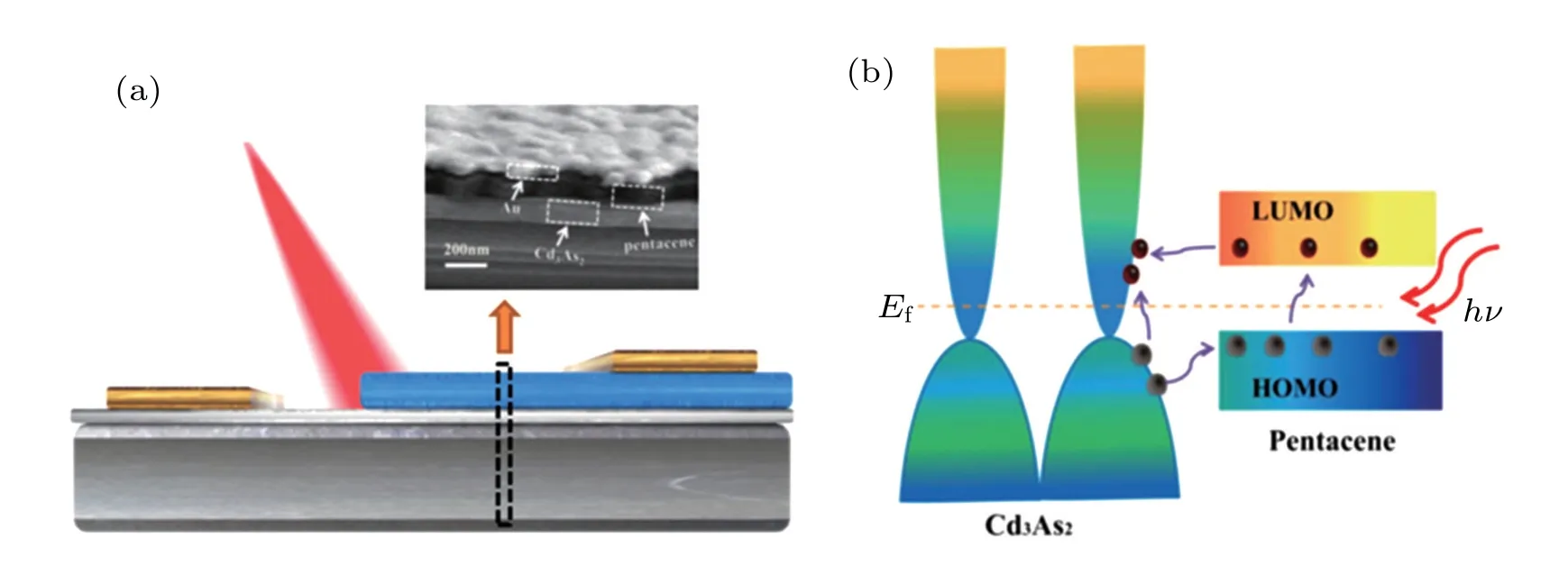
Fig.4.(a)Schematic diagram of photocurrent measurement of Cd3As2/pentacene heterojunction and transmission electron microscopy(TEM)diagram for the cross-section view.(b)Energy-band diagrams of ideal Cd3As2/pentacene heterojunction,where LUMO means the lowest unoccupied molecular orbital and HOMO means the highest occupied molecular orbital.This figure is partially adapted from Ref.[39],ACS Publications Group.

Fig.5.(a)I–V curves of the Cd3As2 thin film/pentacene heterojunction photodetector with and without illumination at the wavelength of 650 nm.(b)and(c)Photocurrent curves of Cd3As2/pentacene heterojunction measured under different wavelengths without and with bias voltage,respectively.(d)Photocurrent curves with bias voltage at wavelengths of 450,520,650,780,980,1310,and 1550 nm.(e)Comparison between responsivity(Ri)of Cd3As2 thin films/pentacene heterojunction photodetector and Cd3As2 thin film photodetector.(f)Wavelength-dependent EQE of Cd3As2/pentacene heterojunction photodetectors.This figure is adapted from Ref.[39],ACS Publications Group.
Compared with the pure Cd3As2photodetector, the Cd3As2/pentacene photodetectors achieve an obvious improvement of Ri. The pentacene layer plays important roles in both the visible band and the infrared band.It has a good absorption in the visible spectrum,which means that it can absorb the light and then produce charges when the light is incident in the junction area of pentacene and Cd3As2.Thus,the Riof the Cd3As2/pentacene heterostructure detector is much higher than that of the pure Cd3As2thin film detector in the visible band. Since pentacene has proved to have a single peak exciton fission effect at about 660 nm,more conductive charges are generated when the light irradiates,which causes Rito reach a maximum value at 650 nm.As a result,the Rivalue of the Cd3As2/pentacene detector is also higher than that of the pure Cd3As2thin film detector in the infrared band.
3.3.Cd3As2 mid-infrared optical switches
Since the early 1990 s,semiconductor saturable absorber mirrors(SESAMs)have been an important approach in the near-infrared field.Flexibility and preciseness make SESAMs one of the most important saturating absorber technologies,and it can be adapted into various laser formats,such as fibre,solid-state or semiconductor chip lasers.[43–45]By detecting the mid-infrared optical response of the bulk Dirac fermions,it is found that MBE-grown Cd3As2thin films can act as an excellent ultra-fast(<10 ps)optical switch in the mid-infrared,with a working range covering at least 3µm–6µm.
We carry out pump-probe measurements on the intrinsic and Cr-doped Cd3As2thin films. The non-degenerate transient transmission spectroscopy reveals photo-bleaching characteristics caused by Pauli blockage,according to which we show that Cd3As2has a saturated absorption characteristics over the entire spectral range(Fig.6(a)).We summarize all the fitted time constants in Fig.6(b),which clearly shows that MBE-grown Cd3As2films exhibit ultrafast saturated absorption at mid-infrared wavelengths ranging from 3µm to 6µm. Figure 6(c)displays the power-dependent transmittance of Cd3As2thin film. Here,the transmittance is determined from T(l)=1 −∆T·exp[−I/Isat]−Tns,where I,Isat,∆T,and Tnsrespectively denote input intensity,saturation intensity,modulation depth,and non-saturable absorbance. A simple saturation model[46]can fit the measurement data.As shown in Fig.6(c),this system can yield a modulation depth of ∼4.4%.In addition,the powerful parametric customization of the Cd3As2allows the on-demand access to different pulse states in 3-µm fiber laser,indicating the potential for a significant increase in the performance level of mid-infrared pulsed laser.Compared with some lasers made of low-dimensional materials such as graphene and black phosphorus,[47,48]the laser made of Cd3As2film possesses advantages,such as scaling to longer mid-infrared wavelength as well as flexibility in customizing the relaxation time.
To illustrate the benefits of expanding the parameter space through a delicate Cr doping,we demonstrate on-demand access to different pulse states for domestic 3-µm fluoride fiber lasers using Cd3As2films with different relaxation times.A fiber laser test bench is chosen,and the demonstration can also be carried out on other mid-infrared lasers,such as an extracavity semiconductor laser.The pulsed laser setup is shown in Fig.7(a).Firstly,we use an un-doped Cd3As2film with a relatively long time constant(∼7 ps at a wavelength of ∼3µm).As can be seen from Fig.7(b),it appears that the continuous wave(CW)emission becomes the Q-switched mode-lock envelope when the pump power reaches 58 mW.

Fig.6.(a)Non-degraded ultrafast pump-probe results at probe wavelengths between 3µm and 6µm,and solid red line corresponding to single exponential fit of τnondeg.(b)Fitted plots of relaxation time constant τ versus probing wavelength for both degenerate(black and red points)and non-degenerate(blue points)measurements.(c)Nonlinear absorption at wavelength 3µm(black points)and fitting with simple saturation model(red line).This figure is adapted from Ref.[40],Nature Publishing Group.

Fig.7.(a)Schematic diagram of fibre laser setup,where LD,PBS,and DM are diode laser,polarized beam splitter,and dichroic mirror,respectively.(b)Q-switched mode-locked pulses at pump power 57.6 mW.(c)CW mode-locked(CWML)pulses at pump power 286.9 mW.No discernable envelope modulation indicates stable operation.(d)Output optical spectrum.Because reduction in intracavity loss results in a lower initial Stark manifold of the 5I6 level,center wavelength of continuous wave operation is red-shifted to 2864.3 nm.At the same time,since required spectral Fourier component is small,the full width at a half maximum reduces to 1.7 nm.(e)Radio frequency(RF)spectra have scan range 0.8 MHz and resolution bandwidth 10 kHz,with repetition rate and signal-to-noise ratios being 14.28 MHz and 54 dB,respectively.Inset shows RF spectra with broader scans ranging from 0 to 160 MHz.(f)Autocorrelation curve measured with intensity autocorrelator.Blue points are experimental results,and red line refers to the fitting results from sech function.This figure is adapted from Ref.[40],Nature Publishing Group.
As the pump power further increases,the duration and period of the Q-switched envelope both shorten as expected.As displayed in Fig.7(c),the Q-switched mode-locking state quickly changes into CW mode-locking when the pump power becomes 80 mW,and the pump power can be maintained up to 290 mW.The pulse period of 70 ns is consistent with the calculated cavity round trip time.Figure 7(d)displays the optical spectrum of the mode-locked pulses.The center wavelength can reach 2860 nm and the FWHM can be 6.2 nm. Moreover,as shown in Fig.7(e),the radio-frequency spectra of the pulses are also measured to determine a robust and stable mode-locking operation.Figure 7(f)shows that the pulse duration is measured by using a home-made mid-infrared autocorrelator and the pulse width is estimated at 6.3 ps. It is clear that un-doped sample could achieve stable mode locking.The Cr-doped Cd3As2film with a shorter relaxation time is then introduced into the cavity in turn.It is found that as the relaxation time of Cd3As2is shortened,the threshold for CW mode-locking increases because the higher intensity is now required to saturate the conduction band.
4.Conclusions and perspectives
Cd3As2, as a topological Dirac semimetal in threedimensionality,has shown a quantum Hall effect(QHE)in both nanostructures and thin films.[49–51]Particularly, our group has reported the 3D Weyl-orbit-based QHE in Cd3As2nanoplates.[52]Hence,with the mobility increasing,it is hopeful to achieve high-quality thin films in the quantum Hall regime.In this regard,the Zn doping can validly reduce the Fermi level,which makes the films easier to reach the quantum limit. Therefore,the electron–electron interactions can be significantly enhanced as demonstrated by several recent experiments on the phase transitions of several topological semimetals.[53,54]Thus,it is quite exciting to continue improving the crystalline quantity of Cd3As2films as well as the effective Zn doping,to envisage the exotic 3D quantum behavior in topological semimetal systems.
While the fundamental research on new topological physics and the various emergent phenomena continue to be conducted,we attempt the potential utilization of topological properties in practice.The Cd3As2has proved to have an extraordinary optical response. Since the Cd3As2/pentacene heterojunction device can raise the responsivity and external quantum efficiency in a broad range from visible light to far-infrared light,it is feasible to use the heterostructures of Cd3As2and organic molecules to construct the photodetectors.Along this route,we expect to realize the devices with higher responsivity and external quantum efficiency with different organic molecules,and make the responsive range much broader(towards THz).[55]Considering the excellent broadband responsiveness of these Cd3As2/organic thin film photodetectors,our work provides a new approach to applying the 3D TDSs to optoelectronic devices.
Furthermore,the attempt of using Cd3As2as a saturable absorber in the field of pulsed lasers seems to be quite successful. The key characteristics including comprehensive scalability,broadband operation,and flexible parameter control effectively establish Cd3As2as a highly adaptable near-infrared SESAM.[56–58]In development,we anticipate the proposed electrically contacted saturable absorber device.It can be further extended to active photonic devices operating in the nearto far-infrared range,including optical modulators and tunable light-emitting devices.
In short,our research on high-quality Cd3As2thin films paves the way for applying the 3D TDSs to photodetectors and presents a feasible approach to preparing the large-scale array photodetectors.Meanwhile,our work represents a step forward in the development of compact mid-infrared ultrafast sources for advanced sensing,communication,spectroscopy,and medical diagnostics using topological Dirac semimetal materials.
猜你喜欢
红蜻蜓·低年级(2021年9期)2021-09-22
红蜻蜓·低年级(2021年8期)2021-08-23
好孩子画报(2020年5期)2020-06-27
音乐天地(音乐创作版)(2019年10期)2020-01-06
活力(2019年19期)2020-01-06
作文周刊·小学一年级版(2019年32期)2019-10-15
作文周刊·小学二年级版(2019年32期)2019-10-15
作文周刊·小学二年级版(2019年28期)2019-09-06
中华建设(2019年4期)2019-07-10

- Chinese Physics B的其它文章
- Compact finite difference schemes for the backward fractional Feynman–Kac equation with fractional substantial derivative*
- Exact solutions of a(2+1)-dimensional extended shallow water wave equation∗
- Lump-type solutions of a generalized Kadomtsev–Petviashvili equation in(3+1)-dimensions∗
- Time evolution of angular momentum coherent state derived by virtue of entangled state representation and a new binomial theorem∗
- Boundary states for entanglement robustness under dephasing and bit flip channels*
- Manipulating transition of a two-component Bose–Einstein condensate with a weak δ-shaped laser∗