
Electron tunneling through double-electric barriers on HgTe/CdTe heterostructure interface
2022-11-21 09:37LiangZhongLin林亮中YiYunLing凌艺纭DongZhang张东andZhenHuaWu吴振华
Chinese Physics B 2022年11期
Liang-Zhong Lin(林亮中) Yi-Yun Ling(凌艺纭) Dong Zhang(张东) and Zhen-Hua Wu(吴振华)
1School of Information Engineering,Zhongshan Polytechnic,Zhongshan 528400,China
2School of Physics and Material Sciences,Guangzhou University,Guangzhou 510000,China
3SKLSM,Institute of Semiconductors,Chinese Academy of Sciences,Beijing 100083,China
4MEDIT,Institute of Microelectronics,Chinese Academy of Sciences,Beijing 100029,China
We investigate theoretically the carrier transport in a two-dimensional topological insulator of (001) HgTe/CdTe quantum-well heterostructure with inverted band, and find distinct switchable features of the transmission spectra in the topological edge states by designing the double-electric modulation potentials. The transmission spectra exhibit the significant Fabry–P´erot resonances for the double-electric transport system. Furthermore, the transmission properties show rich behaviors when the Fermi energy lies in the different locations in the energy spectrum and the double-electric barrier regions. The opacity and transparency of the double-modulated barrier regions can be controlled by tuning the modulated potentials,Fermi energy and the length of modulated regions. This electrical switching behavior can be realized by tuning the voltages applied on the metal gates. The Fabry–P´erot resonances leads to oscillations in the transmission which can be observed in experimentally. This electric modulated-mechanism provides us a realistic way to switch the transmission in edge states which can be constructed in low-power information processing devices.
Keywords: HgTe/CdTe quantum well, double-electric modulations, transmission spectra, Fabry–P´erot resonances
1. Introduction
Topological insulators (TIs) are a new class of materials that have been theoretically predicted[1–6]and demonstrated experimentally.[7–10]They are band insulators (BIs) in the bulk while conducting along the surfaces, possessing surface states with a spin texture protected by time-reversal symmetry. This kind of electron transport is robust against the nonmagnetic impurity scattering and local perturbation.[11–14]The concept of a topological insulator dates back to the work of Kane and Mele, who focused on two-dimensional (2D)systems.[1,2]The spin texture induced by spin–orbit interaction (SOI) in non-centrosymmetric materials has been regarded as a promising avenue for next-generation spintronics applications.[15–19]This offers great potential applications in a new generation of spintronic devices for low-power information processing.[20–24]
In 2D HgTe/CdTe quantum wells(QWs)with an invertedband structure, the helical edge channels have been demonstrated experimentally in the Hall bar geometry.[7,8]There is plenty of research about the potential applications based on construct improved devices in HgTe and various TI material systems.[25–31]As a basic building block of the electric devices, the electric metal strip modulations have been studied extensively in various systems.[32–34]This offers great potential for a new generation of spintronic devices with low-power information processing. A crucial step in this development is the (preferentially electrical) manipulation, i.e., switch on or off, of the channel transport. Therefore, electrical manipulation of the transport property of TIs becomes one of the central issues in the condensed matter physics.It is highly desirable to achieve an electric control of the carrier transport related with this new class of materials.
In this work,we are particularly interested in HgTe/CdTe QWs because HgTe/CdTe is the first TI discovered in nature.[7,8]We investigate theoretically the carrier transport properties through the HgTe/CdTe QW heterostructure under double-electric modulations. The modulation potential can be controlled by the external voltages applied on the metal gate. As will be seen, rich transmission features will shown by changing the double-electric modulated parameters. Different transport processes can be achieved by tuning the modulations potential. The Fabry–P´erot resonances[32–35]can be observed due to the interference between double modulated regions.The transmission shows the Fabry–P´erot resonances for the inter-band tunneling process and is blocked for the intraband process. The constructive interference of the backscattering by double modulations layers will lead to the block of transmission. Furthermore, the bulk gap of HgTe/CdTe QWs can be used to switch off the system. The transport property of the propagating states can also be controlled by the length of modulated regions.
2. Model and formulations
We consider a HgTe/CdTe QW heterostructure with double-electric-modulation structures in planar geometry [as shown schematically in Fig.1(a)]. A voltage gate is deposited on top of the heterostructure to create an electric modulation with biasVg.[32,33]For simplicity,each electric potential is assumed to be of a step-like profile, i.e.,V=Vgin the modulated region andV=0 otherwise. The electric modulation amplitudee·Vgcan be tuned by adjusting the top gate voltage. The carriers injected from left lead can transmit or reflected under the double-electric modulated regions. An effective four-band model introduced by Bernevig,Hughes and Zhang (BHZ-model)[7,8]consists of two disconnected blocks(including twoΓ6electron bands|e ↑〉,|e ↓〉and twoΓ8heavy hole bands|hh ↑〉,|hh ↓〉by neglecting the light-hole and spinsplit bands). The BHZ-model adequately describes the insulating regime in HgTe/CdTe QWs close to theΓpoint and the topological quantum phase transition near the critical thicknessd=dc. The carriers states in the low-energy regime can be well described by a four-band effective HamiltonianH0.In the presence of the double-electrical modulated potentials,the total 4×4 Hamiltonian in the basis|e ↑〉,|hh ↑〉,|e ↓〉,and|hh ↓〉can be written asH=H0+Vg1+Vg2,withH0given by[7]
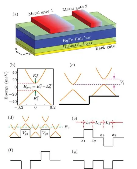
Fig. 1. (a) Schematic illustration of HgTe/CdTe QW heterostructure planar geometry with double gate-induced barriers created by two metallic strips on the surface. (b)The energy spectra for the considered HgTe/CdTe QW system. ETe is the lowest energy of the conductionband(locates at the position E=10 meV)and ETh is the highest energy of the valance-band (locates at the position E =-10 meV) of the energy dispersion. Thus, Egap =ETe -ETh =20 meV is the bulk gap of the system. (c) Schematic illustration of the Egap shifted upwards Vg by the metal gate modulation potential. (d)–(g)Different configurations for the delta-function-shaped electric modulations. Vg1 and Vg2 indicate the electric modulation potential. L1 and L2 indicate the length of the first and second modulated region, respectively. L12 represents the length between double electric modulated regions. The energy dispersions in the different regions of the system shown in (d), and the horizontal dashed line indicates the Fermi energy EF.


Herexλ(λ=1,2,3,4)indicate the interfaces coordinates andj(=1,...,5) represent the transverse discretized strips (especially, whenj= 1 and 5 denote the left lead and right lead,respectively). By scattering matrix theory,[23]we obtain the total transmission probability from the Landauer–B¨uttiker formula[38,39]
where the sum runs over all right-moving modes in the left and right leads.
3. Results and discussion
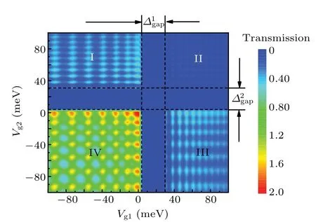
Fig. 2. Contour plot for the total transmission probability T(Vg1,Vg2)of transmitted carrier as functions of double-electric modulations amplitude Vg1 and Vg2 for fixed Fermi energy EF=15 meV and incidence angle θ =π/4. If not specified,L1=L2=L12=100 nm.
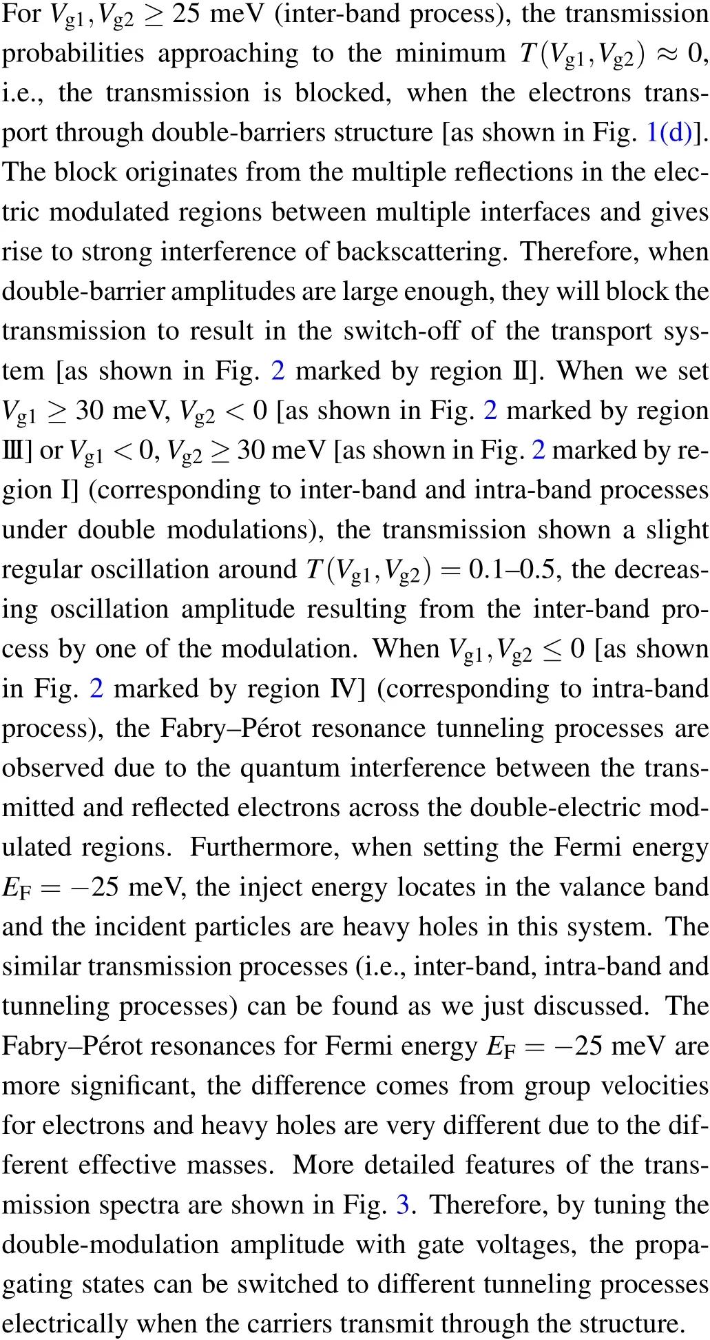
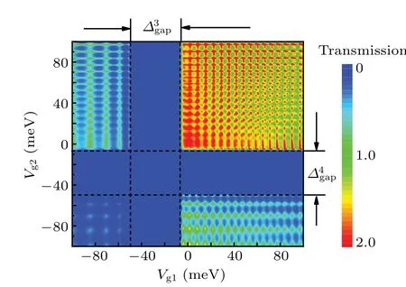
Fig.3. Contour plot for the total transmission probability T(Vg1,Vg2)of transmitted carrier as functions of double-electric modulations amplitude Vg1 and Vg2 for fixed Fermi energy EF =-25 meV and incidence angle θ =π/4.


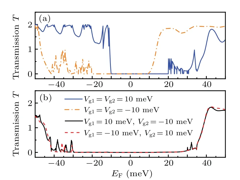
Fig. 4. The total transmission probability T as a function of Fermi energy EF (for fixed gate voltage Vg1 and Vg2 and incidence angle θ =π/4)for different-electric-modulation configurations[as indicated by different color lines(a)and(b)]. The blue solid,orange dashed-dot,black solid, and red dashed lines correspond to the configurations in Figs.1(d)–1(g),respectively.
In Fig. 5, we show the total transmissionT(L12) variations with the distance between two applied biases for fixed Fermi energy and the electric potential. The Fermi energyEF=-15 meV locates in the valance band,the transmission is oscillating regularly with the distanceL12for fixedVg1=Vg2=10 meV[as shown by black solid line in Fig.5(a)].The oscillation originates from the Fabry–P´erot interference between the transmitted and reflected carriers in the electric modulated regions.The same oscillation of transmission can be found when Fermi energyEF= 15 meV locates in the conduction-band for modulations potentialVg1=Vg2=-10 meV[as shown by orange dashed line in Fig. 5(a)]. The oscillation arises from the same mechanism, e.g., the Fabry–P´erot resonances tunneling process. Furthermore, the transmission shows a slight oscillation aroundT(L12)=0.07–0.12 for the anti-parallelmodulation configurations [corresponding to Figs. 1(e) and 1(f)] as clearly reflected in Fig. 5(b). The electric barrier in the anti-parallel-modulation configurations leading to the constructive interference of backscattering from double modulations layers, resulting in the decreasing transmission amplitude. We can expect that the transmission spectra in the configurations of two different anti-parallel modulations will complete coincidence with each other, this is confirmed in Fig.5(b).
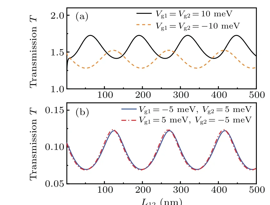
Fig.5. The total transmission probability T as a function of the length between double electric modulated regions L12 with fixed incidence angle θ =π/4 and electric modulations potential. (a) The black solid and orange dashed lines corresponding to EF=-15 meV,Vg1=Vg2=10 meV and EF =15 meV, Vg1 =Vg2 =-10 meV, respectively. (b)For a given Fermi energy EF=15 meV,located in the conduction band.The blue solid and red dashed-dot lines correspond to Vg1 =-5 meV,Vg2=5 meV and Vg1=5 meV,Vg2=-5 meV,respectively.
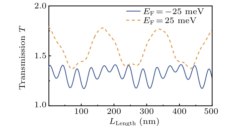
Fig.7. The total transmission probability T as the length of the doubleelectric modulated regions Llength(Llength=L1=L2)for fixed gate voltage Vg1=-5 meV and Vg2=5 meV and incidence angle θ =π/4. The blue solid and orange dashed lines correspond to EF =-25 meV and EF=25 meV,respectively.
Finally we study the transmissionT(Llength)as functions of the length of the double-electric modulated regionsL1andL2for one of the anti-parallel modulation confgiuration structure[as schematic illustrated in Fig.1(f)]. The transmission oscillate periodically with the increasing lengthLlengthfor fxied incidence angle and Fermi energy (as shown in Fig. 7).The anti-parallel modulation confgiuration induces a series of resonances in the transmission spectrum (as shown in Fig. 7.These resonant peaks come from Fabry–Pe´rot resonances in the electric modulated regions at a proper incident angle for a fxied Fermi wave vector. The interference between the transmitted and reflected electrons leads to a series of Fano resonances in the transmissions spectrum. For the other antiparallel modulation confgiuration structure [as schematic illustrated in Fig. 1(e)], we can expect the same transmission spectra for the two anti-parallel modulation configurations as we discussed in the above subsection.
4. Conclusions
In summary,we have investigated theoretically the transport properties of carriers through inverted-band HgTe/CdTe QW topological interface states by double-electric barrier modulations, and found distinct switchable features of the transmission spectra by adjusting the double-electric modulation potentials. The opacity and transparency of the doublemodulated regions can be controlled by tuning the modulated potentials,Fermi energy and the length of modulated regions.The Fabry–P´erot resonances lead to a series of oscillation in the transmission which can be observed experimentally. This electrical switching behavior can be manipulated by tuning the voltages applied on the metal gates. It may pave a way to manipulate the transmission to constructing low-power information processing devices by all electrical way.
Acknowledgements
Project supported by the College Innovation Project of Guangdong Province (Grant No. 2020KTSCX329), the Social Public Welfare and Basic Research Project of Zhongshan City (Grant No. 2020B2044), Zhongshan Polytechnic Highlevel Talents Project (Grant No. KYG2102), the National Key R&D Program of China (Grant No. 2021YFA1200502),and the National Natural Science Foundation of China(Grant No.12174423).

- Chinese Physics B的其它文章
- A design of resonant cavity with an improved coupling-adjusting mechanism for the W-band EPR spectrometer
- Photoreflectance system based on vacuum ultraviolet laser at 177.3 nm
- Topological photonic states in gyromagnetic photonic crystals:Physics,properties,and applications
- Structure of continuous matrix product operator for transverse field Ising model: An analytic and numerical study
- Riemann–Hilbert approach and N double-pole solutions for a nonlinear Schr¨odinger-type equation
- Diffusion dynamics in branched spherical structure