
Investigation of transport properties of perovskite single crystals by pulsed and DC bias transient current technique
2022-11-21 09:29JuanQin秦娟GangCao曹港RunXu徐闰JingLin林婧HuaMeng孟华WenZhenWang王文贞ZiYeHong洪子叶JianCongCai蔡健聪andDongMeiLi李冬梅
Chinese Physics B 2022年11期
Juan Qin(秦娟) Gang Cao(曹港) Run Xu(徐闰) Jing Lin(林婧) Hua Meng(孟华) Wen-Zhen Wang(王文贞) Zi-Ye Hong(洪子叶) Jian-Cong Cai(蔡健聪) and Dong-Mei Li(李冬梅)
1School of Materials Science and Engineering,Shanghai University,Shanghai 200444,China
2Zhejiang Institute of Advanced Materials,Shanghai University,Jiashan 314113,China
Time-of-flight(ToF)transient current method is an important technique to study the transport characteristics of semiconductors. Here, both the direct current (DC) and pulsed bias ToF transient current method are employed to investigate the transport properties and electric field distribution inside the MAPbI3 single crystal detector. Owing to the almost homogeneous electric field built inside the detector during pulsed bias ToF measurement,the free hole mobility can be directly calculated to be about 22 cm2·V-1·s-1,and the hole lifetime is around 6.5 μs–17.5 μs.Hence,the mobility-lifetime product can be derived to be 1.4×10⁻⁴ cm2·V-1–3.9×10⁻⁴ cm2·V-1. The transit time measured under the DC bias deviates with increasing voltage compared with that under the pulsed bias, which arises mainly from the inhomogeneous electric field distribution inside the perovskite. The positive space charge density can then be deduced to increase from 3.1×1010 cm-3 to 6.89×1010 cm-3 in a bias range of 50 V–150 V.The ToF measurement can provide us with a facile way to accurately measure the transport properties of the perovskite single crystals, and is also helpful in obtaining a rough picture of the internal electric field distribution.
Keywords: MAPbI3,space charge density,electric field distribution,time-of-flight measurement
1. Introduction
The remarkable research progress of Halide perovskite materials in optoelectronics have been made[1–3]due to their excellent optical and electrical properties. Of them,the transport behavior of charge carriers is the most essential.[4–9]The mobility and lifetime of charge carriers are the key parameters for transport, and a larger mobility-lifetime product(μτ)leads to a higher charge collection efficiency and a higher sensitivity for detectors. The charge carrier lifetime of perovskite single crystal (PSC) was believed to be longer than that of other semiconductors like CdZnTe (CZT),[5,10]while the mobility of charge carriers was considered to be one order of magnitude smaller than that of CZT,[7,11–14]which might be a hazardous issue for PSC to be utilized in high speed radiation devices. In addition, the reported mobility values of MAPbI3PSC were widely varied in a range of 24 cm2·V-1·s-1–620 cm2·V-1·s-1, by different methods including space charge limited current (SCLC), time of flight(ToF),time-resolved microwave conductivity.[5,10,15]
The ToF method based on transient current is suitable to the PSC with high resistivity, which can directly profile the transport process of non-equilibrium carriers, and precisely measure the transit time and hence the free carrier mobility.Besides, some internal physical information in semiconductors can be derived from current waveforms (CW) of ToF measurement, such as the interaction of carriers with traps and electric field distribution.[16–19]A study of temperaturedependent mobility of MAPbI3by ToF was caried out first in 2018.[20]The characteristics of the trapping-de-trapping of carriers in PSC defects have been clearly uncovered by the pulsed bias ToF method combined with Monte Carlo simulation.[16,21]
However, radiation detection operates practically under the DC bias rather than pulsed bias. The space charge inside the bulk is negligible for the pulsed bias,and the drift transport properties can be different from those under the DC condition with non-negligible space charge. The space charge built up inside the detector under the DC bias may redistribute the electric field and hence retard/accelerate the carrier transport,just as in CdTe and CZT.[22–24]Therefore,to better understand the transport properties of PSC operated under DC bias,the space charge and electric field distribution should be taken into account.
Here, we focus on the transport properties of the PSC detector by using a ToF transient current measurement system. By employing a DC bias ToF measurement and referring to pulse bias results, it can be estimated that the positive space charge density increases from 3.1×1010cm-3to 6.89×1010cm-3as the bias rises from 50 V to 150 V. A free hole mobility of about 22 cm2·V-1·s-1can be calculated directly from the pulsed bias ToF method due to the almost homogeneous electric field built inside the MAPbI3. The hole lifetime measured in the pulsed mode is 6.5 μs–17.5 μs,and hence the mobility-lifetime product can be derived to be 1.4×10⁻⁴cm2·V-1–3.9×10⁻⁴cm2·V-1. By using the DC bias voltage, the transit time of holes in MAPbI3is deviated downward from that under pulsed condition due to the positive space charge and inhomogeneous electric field distribution inside the PSC.
2. Experiment
The MAPbI3PSC was grown by the inverse temperature crystallization (ITC) method and prepared into a size of 5 mm×5 mm×2 mm, then polished on both sides and deposited with 40-nm-thick Au electrodes (Au/MAPbI3/Au).The details can be found in our previous report.[25]

Fig. 1. (a) Schematic diagram of ToF transient current measurement system and (b) schematic time sequence of voltage and laser pulse for a ToF measurement. The top panel illustrates that a typical ToF current waveform can be divided into several characteristic segments, with a “knot” between segment 2 and segment 3,which represents the free carrier transit time.
The ToF transient current measurement system is shown in Fig.1(a),which consists of several apparatuses.The system worked as follows:two signal generators(Keithley 3390)were used to generate two controlled signals sequentially,where the pulse voltage control (Analog Devices LTC 6090) was triggered first,then after a delay time,the laser pulse,which was generated by a 650-nm laser diode (10 mW), was triggered.The current signal in the external circuit was amplified by a current amplifier(ADI LTC6268-10 100 MHz)and sent to oscilloscope (R & S RTE1054 500 MHz, 5 GSa/s) for recording. The laser pulse energy was estimated at 5 nJ(500 ns with 10 mW).
The time sequence configuration of the pulsed bias voltage and laser pulse in ToF measurement are shown in Fig.1(b).For pulsed bias mode,the frequency and width of the voltage pulse were set to be at 20 Hz and 400 μs, respectively. The delay time between the rising edge of pulsed bias and the laser pulse was 50 μs,while the width of the laser pulse was 500 ns.For DC bias mode,the frequency and width of laser pulse were required to be the same as those for pulsed bias mode.
3. Results and discussion
We have measured the ToF CWs for holes under both DC and pulsed bias mode,and the results are displayed in Fig.2.Similar ToF CWs containing all the characteristic segments(Fig. 1(b)) for both modes can be observed. The first sharp rise is attributed to laser pulse excitation. Then,a drop of current occurs as illustrated by segment 1 in Fig.1(b),which can be related to the surface recombination[17]and/or trapping of generated carriers.[16]Surprisingly, the current then tends to increase to another peak within a few microseconds.This phenomenon can be observed for all of our samples,as well as in some reports about PSC and even CZT.[19,20,26]This abnormal increase may arise from the electric field distortion of carriers,as these carriers are highly concentrated in a finite space and separated instantaneously,[20]or due to the presence of surface traps at the interface of MAPbI3,forming depletion zones and possibly acting as pn junctions or“dead(inactive)layers”.[22]During ToF measurement,this unusual rise of current after the first current drop may show a fake knot in CW,which can result in the wrong estimation of mobility if assuming the“knot”position to serve as the transit time.
When the induced current passes through the second peak value,the curve becomes the same as a typical ToF CW(segment 2 in Fig.1(b)),exhibiting an exponential decay curve related to both the trapping and de-trapping of holes and the electric field distribution inside the semiconductor.[16,17]When the free hole cloud begins to arrive at the cathode,the CW exhibits a turning point called“knot”(knot in Fig.1). So,the knot represents the transit time of free holes.[16,27]
We then focus on the main differences in ToF CW between the pulsed mode and the DC mode,which can beyreflected mainly at the knot position. Note that the space charge density inside the PSC is negligible for pulsed bias due to a very short delay time of 50 μs. Therefore, a transit time for DC ToF longer than that for pulsed ToF at the same bias voltage amplitude can be observed,which indicates the existence of an inhomogeneous electrical field distribution inside a DC bias detector.
Therefore, for a pulsed mode, since the electric field is homogeneous,the value of hole mobility can be calculated by using the following simple expression:


Fig.2. (a)DC and(b)pulsed ToF current waveforms at different bias voltages for a 0.2-cm-thick MAPbI3 single crystal detector.
In Fig.3(a),the reciprocal of the transit time as a function of bias voltage under both DC and puled modes is displayed,where the value of the transit time (i.e.the knot position, or the intersection of the segment 2 and segment 3) is extracted from ToF CWs in Fig.2.The reciprocal of transit time exhibits a good linearity with bias voltage in the pulsed mode, which confirms that the electric field in the pulsed mode is almost homogeneous, and therefore can be reliably used to calculate the free hole mobility of MAPbI3to be 22 cm2·V-1·s-1,well in agreement with reported pulse ToF results.[21,28]As listed in Table 1,the mobility values of MAPbI3exhibit a large variation by the SCLC technique and Hall technique. It is difficult to accurately derive mobility from both SCLC and Hall measurements,since the SCLC model requires an ideal Ohmic injecting contact[29]while Hall measurements are also based on Ohmic contact and are inaccurate for high resistivity materials.In contrast, the ToF method can provide consistent mobility values with a relatively small variation,and our result matches
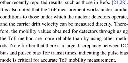

Fig.3. (a)Plot of reciprocal of transit time versus bias voltage from pulsed(blue squares) and DC (black dots) ToF measurements, with green line denoting a linear fit to the data from pulsed mode,from which the hole mobility can be calculated to be 22 m2·V-1·s-1. (b)Plot of effect of different electric field gradients on transit time for a DC bias ToF measurement with gradient a assumed to keep constant for all bias voltages. The transit time is calculated from Eq.(2)by setting L=0.2 cm,μ =22 cm2·V-1·s-1.
For the DC mode,the space charge density and the electric field distribution must be considered after the dielectric relaxation has been achieved. To simplify the physical model,we neglect the effect of the dead layer and assume a linear electric fieldE(x)inside a DC bias detector due to a homogeneous distribution of ionized impurities. A mathematical expression of transit time and voltage at a fixed electric field gradient can been deduced, which has been reported previously as follows:[37,38]


Table 1. Summary of experimentally determined hole charge carrier mobility for MAPbI3 single crystals,all measured at room temperature.

A possible explanation to this discrepancy is that the electric field gradient,i.e.a,is not a constant as described above,but rather should change with bias voltage. From Eq.(3),we can see that the parameterais determined by the space charge density, and hence it can be assumed that the space charge density can vary with bias voltage. Moreover,since the curve for the DC ToF measurement in Fig.3(a)is gradually deviated downward as compared with that for the pulsed ToF, much more impurities are supposed to be ionized at higher bias voltages, leading to a larger gradient of electric field and thereby a longer transit time than that in homogeneous electrical field under the same bias voltage amplitude. Similar cases in CZT have been reported,and the ToF results also showed a change in electric field gradient with bias voltage,[26,37]indicating increased ionized impurities.
From Eqs.(1)and(2) it follows that the transit time under a linear electric field is always longer than that under a constant electric field,whether the electrical field gradientais positive or negative. So, we cannot know whether the space charge is negative or positive. Rather,we find that the induced charges in the DC mode,which can be integrated directly from the ToF CWs, is always around 5% lower than those in the pulse mode under the same bias voltages. For instance, the induced charge in the DC mode is around 21.3 pC as compared with 20.3 pC in the pulse mode under a bias of 150 V.Based on a longer decay characteristic in the DC mode to be discussed below, a lower induced charge density indicates a lower electric field at anode,resulting from the positive space charge distribution inside the detector,which is demonstrated schematically in Fig.4(a).Besides,that the transient current in the DC mode is lower than that in the pulsed mode at the very initial stage under the same voltage also implies a lower electric field at anode. Moreover, this positive space charge can originate most probably from the ionized deep-level donors.
Fig. 4. (a) Schematic diagram of positive space charge and electric field distribution inside the detector, with the light blue background tighter with the red line representing electric field strength. (b) The lifetime of pulsed mode (black dots) and DC mode (red dots) ToF hole carriers, calculated from fitting segment 2 of ToF current waveforms.
As discussed in Fig.1(b),segment 2 of ToF CW exhibits the exponential decay of holes,and therefore Fig.4(b)shows the hole decay constant as a function of bias voltage under pulsed mode and DC mode, which is obtained by fitting segment 2 of ToF CWs. It can be seen that for both modes, the decay constant decreases with bias increasing,which probably originates from the larger excess carriers due to an increased electric field for the splitting of electron–hole pairs at the very initial stage. The decay constant ranging between 6.7 μs and 17.5 μs in the pulsed mode is just the so-called hole lifetime determined by trapping process and de-trapping process of holes in the pulse,and hence the mobility-lifetime product can be derived to be 1.4×10⁻⁴cm2·V-1–3.9×10⁻⁴cm2·V-1,which is well consistent with that from the alpha-particle measurement.[39]The decay constant in the DC mode is determined not only by the hole lifetime,but also by the electric field gradient,[37]according to the following formula:

So, if we assume that the lifetime for the DC mode is the same as that for the pulsed mode, the electric field gradient can be extracted to be 1200 V/cm2–3000 V/cm2, and as the bias voltage increases from 50 V to 150 V,the corresponding positive space charge can then be estimated to increase from 3.1×1010cm-3to 6.89×1010cm-3. This phenomenon that the space charge density increases with bias increasing is well consistent with the above conclusion deduced from the transit time evolution in the DC mode.
4. Conclusions
In this work, the transport properties of the MAPbI3single crystal detector are investigated by both the DC bias ToF transient current method and the pulsed bias ToF transient current method. A free hole mobility of about 22 cm2·V-1·s-1and the hole lifetime of 6.7 μs–17.5 μs can be calculated directly from the pulsed bias ToF method,and hence the mobility-lifetime product can be derived to be 1.4×10⁻⁴cm2·V-1–3.9×10⁻⁴cm2·V-1. Owing to the presence of positive space charge inside the PSC,the transit time measured under the DC bias mode is deviated downward with voltage increasing in comparison with that under the pulsed bias mode. The positive space charge can be estimated to increase from 3.1×1010cm-3to 6.89×1010cm-3with bias increasing from 50 V to 150 V. The DC and pulsed bias ToF measurement methods prove to be reliable methods of accurately measuring the transport properties of the perovskite single crystal under the detector operating conditions.
Acknowledgements
Project supported by the National Natural Science Foundation of China (Grant Nos. 12175131 and 11905133)and the China Postdoctoral Science Foundation (Grant No.2021M692021).
猜你喜欢
小学生作文(低年级适用)(2021年10期)2021-10-29
装备环境工程(2020年5期)2020-06-04
湖北农业科学(2017年6期)2017-04-26
喜剧世界(2016年2期)2016-11-26
百姓生活(2016年4期)2016-10-26
江苏农业科学(2015年11期)2016-01-27
山东农业科学(2015年3期)2015-05-06
长江蔬菜·学术版(2014年7期)2015-01-21
文苑(2011年3期)2011-09-28
中国民族民间医药·下半月(2011年4期)2011-09-27

- Chinese Physics B的其它文章
- A design of resonant cavity with an improved coupling-adjusting mechanism for the W-band EPR spectrometer
- Photoreflectance system based on vacuum ultraviolet laser at 177.3 nm
- Topological photonic states in gyromagnetic photonic crystals:Physics,properties,and applications
- Structure of continuous matrix product operator for transverse field Ising model: An analytic and numerical study
- Riemann–Hilbert approach and N double-pole solutions for a nonlinear Schr¨odinger-type equation
- Diffusion dynamics in branched spherical structure