
A novel Si-rich SiN bilayer passivation with thin-barrier AlGaN/GaN HEMTs for high performance millimeter-wave applications
2022-11-21 09:37ZhihongChen陈治宏MinhanMi宓珉瀚JielongLiu刘捷龙PengfeiWang王鹏飞YuweiZhou周雨威MengZhang张濛XiaohuaMa马晓华andYueHao郝跃
Chinese Physics B 2022年11期
Zhihong Chen(陈治宏) Minhan Mi(宓珉瀚) Jielong Liu(刘捷龙) Pengfei Wang(王鹏飞)Yuwei Zhou(周雨威) Meng Zhang(张濛) Xiaohua Ma(马晓华) and Yue Hao(郝跃)
1Key Laboratory of Wide Band-Gap Semiconductor Materials and Devices,School of Microelectronics,Xidian University,Xi’an 710071,China
2School of Advanced Materials and Nanotechnology,Xidian University,Xi’an 710071,China
3Guangzhou Institute of Technology,Xidian University,Guangzhou 510555,China
We demonstrate a novel Si-rich SiN bilayer passivation technology for AlGaN/GaN high electron mobility transistors(HEMTs)with thin-barrier to minimize surface leakage current to enhance the breakdown voltage.The bilayer SiN with 20-nm Si-rich SiN and 100-nm Si3N4 was deposited by plasma-enhanced chemical vapor deposition(PECVD)after removing 20-nm SiO2 pre-deposition layer. Compared to traditional Si3N4 passivation for thin-barrier AlGaN/GaN HEMTs,Si-rich SiN bilayer passivation can suppress the current collapse ratio from 18.54%to 8.40%. However,Si-rich bilayer passivation leads to a severer surface leakage current, so that it has a low breakdown voltage. The 20-nm SiO2 pre-deposition layer can protect the surface of HEMTs in fabrication process and decrease Ga–O bonds, resulting in a lower surface leakage current. In contrast to passivating Si-rich SiN directly,devices with the novel Si-rich SiN bilayer passivation increase the breakdown voltage from 29 V to 85 V.Radio frequency(RF)small-signal characteristics show that HEMTs with the novel bilayer SiN passivation leads to fT/fmax of 68 GHz/102 GHz. At 30 GHz and VDS =20 V, devices achieve a maximum Pout of 5.2 W/mm and a peak power-added efficiency(PAE)of 42.2%. These results indicate that HEMTs with the novel bilayer SiN passivation can have potential applications in the millimeter-wave range.
Keywords: AlGaN/GaN HEMTs,thin-barrier,Si-rich SiN passivation,current collapse,surface leakage current,millimeter-wave
1. Introduction
Due to the excellent features, such as high breakdown field (3.3 MV/cm), high electron saturation velocity(2.5×107cm/s)and wide bandgap(3.4 eV),GaN-based high electron mobility transistors (HEMTs) have potential in radio frequency (RF) and millimeter-wave applications.[1–4]However, for millimeter-wave devices with thin-barrier, the polarization effect decreases and the concentration of twodimensional electron gas(2DEG)on the GaN side of the Al-GaN/GaN heterojunction interface is much lower than that of the conventional barrier structure, thus the current of the devices is poor and the saturation current is low.[5]In addition,thin-barrier HEMTs have a problem of severe surface leakage current after using the conventional Si3N4passivation process,which can cause the breakdown voltage of the device decrease,as well as the current collapse effect.[6,7]Some reports have confirmed that current collapse is caused by traps on the device surface.[8,9]When the traps locate between gate and drain access region,it will exist a second virtual gate,which will deplete 2DEG.[10–12]With the decrease of barrier thickness,surface traps have more effect for 2DEG in the channel. Because of the increase in the electric fields in thin-barrier HEMTs,current collapse will become more serious.[13]
For ordinary GaN HEMTs,current collapse has been well suppressed in various methods.[14–16]It is no doubt that passivation is the most commonly used way to mitigate current collapse.[17–19]Bilayer SiN passivation technology has been studied in recent reports. This method can not only optimize DC performances like current collapse,but also improve small-and large-signal characteristics because it can be good used to decrease traps-related dispersive effects caused by electron trapping. In 2015,Huanget al.reported that HEMTs with bilayer SiN passivation with Si-rich SiN can decrease the current collapse ratio to 3.31% at quiescent bias points(VGS,Q,VDS,Q)=(-6 V,24 V)and obtained an output power density of 5.4 W/mm at 3 GHz.[20–22]In addition,by contrast to traditional Si3N4passivation film,Si-rich SiN film has relatively more Si–H bonds because of the increasing of SiH4flow.[23]However,as for thin-barrier HEMTs,Si-rich SiN bilayer passivation has only suppressed current collapse in our previous research. Devices have a low breakdown voltage because of severe surface leakage current, which restricts their power application at high voltage.[24]The leakage current may be created by surface traps,which comes from plasma etching during the fabrication process.[25]
In this work, a novel Si-rich SiN bilayer passivation was deposited by plasma-enhanced chemical vapor deposition(PECVD) for AlGaN/GaN HEMTs with thin-barrier. Compared to Si3N4passivation, Si-rich SiN/Si3N4bilayer passivation can not only increase 2DEG density,but also suppress current collapse ratio from 18.54% to 8.40% at the quiescent bias point (VGS,Q,VDS,Q) = (-8 V,30 V). Nevertheless, it had an extremely low breakdown voltage of 29 V and a large surface leakage current. Based on these results, we fabricated HEMTs with Si-rich SiN bilayer passivation after removing SiO2pre-deposition layer. This novel bilayer passivation technology can effectively decrease surface traps and surface leakage current, so that suppress current collapse and enhances the breakdown voltage. The fabricated devices can obtain anfT/fmaxof 68 GHz/102 GHz atVDS= 6 V, and demonstrate an output power density(Pout)of 5.2 W/mm and a peak power-added efficiency(PAE)of 42.2%at 30 GHz andVDS=20 V.The off-state stress measurement results show that HEMTs have nearly no degradation in saturation current and peak transconductance atVgstress=-5 V,Vdstress=40 V andtstress=1000 s, denoting that devices have a long-term reliability. These results indicate that this novel passivation technology can have a good use in millimeter-wave range for thinbarrier AlGaN/GaN HEMTs.
2. Device structure and fabrication
Two types of device schematic cross-sections with Sirich SiN bilayer passivation are exhibited in Fig. 1. Devices in Fig. 1(a) were passivated with 20-nm Si-rich SiN (Si-rich SiN,SiH4:NH3flow=450:2 sccm)and 100-nm Si3N4(Si3N4,SiH4:NH3flow=100:2 sccm). Devices with the novel Si-rich SiN bilayer passivation in Fig. 1(b) were passivated with 20-nm Si-rich SiN and 100-nm Si3N4after removing SiO2predeposition layer. The AlGaN/GaN heterostructure of all devices was epitaxially grown on SiC substrate by metal–organic chemical vapor deposition(MOCVD).And the epilayers were consisted of 1.6-μm GaN buffer, 400-nm i-GaN layer, 1-nm AlN spacer layer,and 12-nm AlGaN barrier layer.

Fig. 1. Schematic diagram of AlGaN/GaN HEMTs with (a) Si-rich SiN bilayer passivation. (b) Si-rich SiN bilayer passivation after removing SiO2 pre-deposition layer.
The only difference in device fabrication of HEMTs with the novel Si-rich SiN bilayer passivation is that it was deposited 20-nm SiO2layer at the first process. Ti/Al/Ni/Au ohmic contact was treated by the electron beam evaporation and rapid temperature annealing (RTA) at 830°C for 60 s in N2ambient. The measured ohmic contact resistance (RC)by transfer line measurement (TLM) was 0.39 Ω·mm. Device isolation was formed by nitrogen ion implantation. Then the SiO2pre-deposition layer was removed using hydrofluoric acid. Si-rich SiN/Si3N4bilayer passivation was then deposited by PECVD. T-shaped gate was defined by electronbeam lithography(EBL),and etched by CF4-based inductively coupled plasma(ICP)etching to remove SiN in the gate-foot.Finally, the Ni/Au gate electrode was deposited by electron beam evaporation. The gate length was 150 nm, the sourcedrain distance was 2 μm,and the gate width was 2×50 μm.
3. Results and discussion
3.1. Current collapse suppression
The DC transfer characteristics and TLM measurement results of AlGaN/GaN HEMTs with traditional Si3N4and Sirich SiN bilayer passivation are shown in Fig. 2. We can see from Fig. 2(a) that HEMTs with Si-rich SiN improved drain current (ID) and peak transconductance (Gm) atVDS= 6 V from 1057 mA/mm and 344 mS/mm to 1273 mA/mm and 408 mS/mm, respectively, compared to HEMTs with Si3N4passivation. These results indicated that Si-rich SiN bilayer passivation could effectively increase 2DEG density,resulting in an improvement for current and transconductance. Meanwhile,as shown in TLM measurement results in Fig.2(b),after passivating Si-rich SiN,Rsheetdecreased from 334 Ω/□to 277 Ω/□. The reduction ofRsheetwas also benefited from the increase of 2DEG density.
On the other hand,Si-rich SiN bilayer passivation solved the current collapse for thin-barrier HEMTs. TheI–Vpulsed characteristics of HEMTs were measured by Keithley-4200 semiconductor parameter analyzer to investigate current collapse in Fig. 3, where the pulse width and pulse period were 500 ns and 1 ms, respectively. The quiescent bias points(VGS,Q,VDS,Q) were set (0 V, 0 V), (-8 V, 0 V), and (-8 V,30 V).We can clearly find that HEMTs with Si3N4passivation had a more serious current collapse ratio about 18.54%at the quiescent bias point(-8 V,30 V).However,after passivating Si-rich SiN bilayer passivation, devices had an excellent current collapse performance. It reached only 0.35%and 8.40%current collapse ratio at the quiescent bias point (-8 V, 0 V)and(-8 V,30 V),respectively.The mechanism of suppressing current collapse by Si-rich SiN passivation is that Si–H bonds are more due to the increased flow of the SiH4. The excess Si–H bonds tend to react with the oxygen elements on the device surface,thus reducing the surface state. The reduction of the surface state suppresses the RF scattering,resulting in the suppression of current collapse.[20,21,23]

Fig. 2. (a) Transfer characteristics of HEMTs with Si3N4 and Si-rich SiN bilayer passivation. (b) TLM measurement results of HEMTs with Si3N4 and Si-rich SiN bilayer passivation.
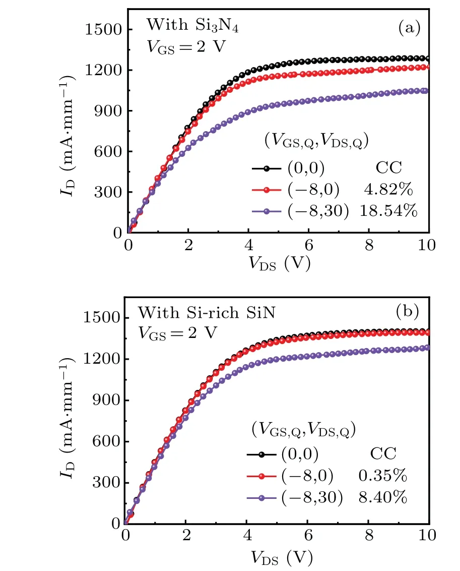
Fig. 3. The I–V pulsed characteristics of AlGaN/GaN HEMTs with (a)Si3N4 passivation. (b)Si-rich SiN bilayer passivation.
3.2. Surface leakage current suppression
To research the effect of SiO2pre-deposition on HEMTs with thin-barrier,we did the same fabrication process by Si3N4passivation layer. The results of devices using four different types of passivation by Si3N4and Si-rich SiN, which were with and without SiO2pre-deposition layer, were shown in Fig.4. It was obvious that HEMTs with Si3N4after SiO2remove still had a high current collapse. It only enhanced the breakdown voltage from 24 V to 81 V. And devices with Sirich SiN after SiO2remove could have a low current collapse and a large breakdown voltage. We will explain the passivation in more detail below.
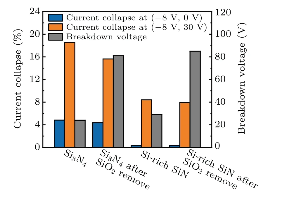
Fig. 4. Comparison of four types SiN passivation on current collapse and breakdown voltage.
Although Si-rich SiN bilayer passivation optimized current collapse for thin-barrier HEMTs, severe surface leakage current caused a very low breakdown voltage. The purpose of the novel bilayer passivation is to suppress surface leakage current. As shown in Fig. 5, after removing SiO2predeposition layer, HEMTs with Si-rich SiN bilayer passivation enhanced the breakdown voltage from 29 V to 85 V atID=1 mA/mm. Dual gate was measured to analyze the mechanism of the enhancement of breakdown voltage. Figure 6 shows the dual gate structure of HEMTs with SiN passivation to distinguish surface leakage current and barrier leakage current. We fabricated another gate 2 by Schottky contact and a negative voltage sweeping was applied to gate 2. On the other hand, source and gate 1 were biased to 0 V, and monitored their current at the same time. It can be seen from the structure that gate 1 had the same potential with 2DEG because ofVgate1=0 V.The leakage current flowed from gate 1 must be surface current,and the barrier leakage current was monitored by the source terminal.[26,27]Figure 7 shows the characteristics of surface leakage current (IS) with gate 2 voltage (VG2)for HEMTs with two types of Si-rich SiN bilayer passivation.As shown in Fig. 7, it was obvious that different SiN passivation could efficiently effect surface leakage current. Compared to passivating Si-rich SiN/Si3N4directly, HEMTs with Si-rich SiN/Si3N4after removing SiO2pre-deposition layer suppressed surface leakage current from 2.5×10⁻³mA/mm to 1.1×10⁻⁶mA/mm atVG2=-50 V.Almost three orders reduction of surface current illustrated that the novel SiN bilayer passivation suppressed the density of surface electronic states and surface leakage current,thereby the breakdown voltage of the HEMTs had a great enhancement.to surface leakage current and breakdown voltage. When the surface traps filled with injected electrons,the depletion region along the channel will be extended,resulting in an electric field peak at the drain-side gate edge.So the surface leakage current and the breakdown voltage have an improvement.[29,30]

Fig. 5. Breakdown voltage (Vbr) comparison of HEMTs with two types of Si-rich SiN bilayer passivation.

Fig. 8. The XPS spectra of Ga 3d for HEMTs with three types of bilayer SiN passivation.

Fig. 7. Surface leakage current (IS) of HEMTs HEMTs with two types of Si-rich SiN bilayer passivation.
The x-ray photoelectron spectroscopy (XPS) was measured to investigate the mechanism of the decrease of surface leakage current and the effect of device surface trap by two types of Si-rich SiN bilayer passivation. Figure 8 shows the Ga 3d core-level spectra of the AlGaN/SiN interface for two samples,respectively.Ga–O bonds and Ga–N bonds were separated from Ga 3d peaks. In contrast to Si-rich SiN sample,the intensity of Ga–O peak in devices with Si-rich SiN after removing SiO2pre-deposition layer had an obvious reduction.The concentration of Ga–O bond in Ga 3d peak can be seen as a marker to qualitatively analyze surface traps content. Thus the decline of Ga–O peak indicates that surface traps was removed by SiO2pre-deposition treatment and passivating Sirich SiN.[28]Meanwhile,surface traps are also closely related
3.3. Small-and large-signal characteristics
The RF small-signal characteristics of HEMTs with the novel bilayer SiN passivation were achieved by Agilent-8363B network analyzer within the frequency from 100 MHz to 40 GHz. The current gain extrinsic cut-off frequency (fT)and the maximum oscillation frequency(fmax)were obtained by short open-load-through calibration standard at 40 GHz.Figure 9 shows the unilateral power gain (UPG), maximum stable gain (MSG), and current gain|H21|2as a function of frequency for sample 3 atVDS=6 V andVGS=-1.8 V.After extrapolating the short circuit current gain(|H21|2)and the unilateral power gain(UPG)curves through using-20 dB/decade slope,thefT/fmaxof sample 3 with Si-rich SiN after removing SiO2had a value offT/fmaxof 68 GHz/102 GHz.

Fig. 9. The RF small-signal characteristics of AlGaN/GaN HEMTs with Si-rich SiN bilayer passivation after removing SiO2 pre-deposition layer.
To verify the application of HEMTs with the novel bilayer SiN passivation in millimeter-wave range and their power characteristics,large-signal power measurement was treated at 30 GHz in continuous-wave(CW)mode. The source and load impedances were tuned to obtain maximum power-added efficiency(PAE).The device was biased at class-AB.AtVDS=20 V,as shown in Fig.10,the PAE,the power gain(gain),and output power density(Pout)were a function of the input power(Pin), respectively. Sample 3 with the novel bilayer SiN passivation had a maximumPoutof 5.2 W/mm and a peak PAE of 42.2%. In millimeter-wave range, the power measurement results demonstrated that HEMTs with the novel bilayer SiN passivation can have excellent applications in Ka-band.
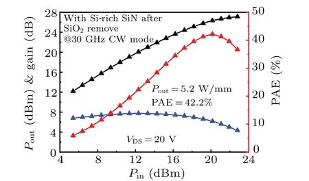
Fig.10. Large-signal characteristics of the HEMTs with Si-rich SiN bilayer passivation after removing SiO2 pre-deposition layer at 30-GHz CW mode.
4. Conclusions
In summary, AlGaN/GaN HEMTs with 20-nm Si-rich SiN and 100-nm Si3N4passivation after removing SiO2pre-deposition layer extraordinarily optimize device performances. This novel bilayer SiN passivation technology solves surface leakage current for thin-barrier GaN-based HEMTs with conventional passivation. HEMTs with this novel passivation can not only suppress current collapse to 8.40% at the quiescent bias point (-8 V, 30 V), but also decrease surface leakage current to 1.1×10⁻⁶mA/mm, so that enhance the breakdown voltage to 85 V.Furthermore,RF small-signal measurement shows that devices with this type of passivation obtainfT/fmaxof 68 GHz/102 GHz. At 30-GHz CW mode,VDS= 20 V, HEMTs have a maximumPoutof 5.2 W/mm and a peak PAE of 42.2%. These results indicate that Al-GaN/GaN HEMTs with the novel Si-rich SiN bilayer passivation technology can have better applications in high voltage and millimeter-wave range.
Acknowledgements
Project supported by the National Key Research and Development Program of China(Grant No.2020YFB1804902),the National Natural Science Foundation of China (Grant Nos. 61904135, 62090014, and 11690042), the Fundamental Research Funds for the Central Universities, the Innovation Fund of Xidian University (Grant No. YJS2213), the China Postdoctoral Science Foundation (Grant Nos. 2018M640957 and BX20200262), the Key Research and Development Program of Guangzhou (Grant No. 202103020002), Wuhu and Xidian University Special Fund for Industry–University-Research Cooperation (Grant No. XWYCXY-012021014-HT), and the Fundamental Research Funds for the Central Universities,China(Grant No.XJS221110).

- Chinese Physics B的其它文章
- A design of resonant cavity with an improved coupling-adjusting mechanism for the W-band EPR spectrometer
- Photoreflectance system based on vacuum ultraviolet laser at 177.3 nm
- Topological photonic states in gyromagnetic photonic crystals:Physics,properties,and applications
- Structure of continuous matrix product operator for transverse field Ising model: An analytic and numerical study
- Riemann–Hilbert approach and N double-pole solutions for a nonlinear Schr¨odinger-type equation
- Diffusion dynamics in branched spherical structure