
A pure dielectric metamaterial absorber with broadband and thin thickness based on a cross-hole array structure
2022-11-21 09:39WenboCao曹文博YouquanWen温又铨ChaoJiang姜超YantaoYu余延涛YiyuWang王艺宇
Chinese Physics B 2022年11期
Wenbo Cao(曹文博) Youquan Wen(温又铨) Chao Jiang(姜超) Yantao Yu(余延涛) Yiyu Wang(王艺宇)
Zheyipei Ma(麻哲乂培)1,2, Zixiang Zhao(赵子翔)1,2, Lanzhi Wang(王兰志)1,2, and Xiaozhong Huang(黄小忠)1,2,‡
1Powder Metallurgy Research Institute,Central South University,Changsha 410083,China
2State Key Laboratory of Powder Metallurgy and Hunan Key Laboratory of Advanced Fibers and Composites,Central South University,Changsha 410083,China
A pure dielectric metamaterial absorber with broadband and thin thickness is proposed,whose structure is designed as a periodic cross-hole array. The pure dielectric metamaterial absorber with high permittivity is prepared by ceramic reinforced polymer composites. Compared with those with low permittivity, the absorber with high permittivity is more sensitive to structural parameters,which means that it is easier to optimize the equivalent electromagnetic parameters and achieve wide impedance matching by altering the size or shape of the unit cell. The optimized metamaterial absorber exhibits reflection loss below-10 dB in 7.93 GHz–35.76 GHz with a thickness of 3.5 mm,which shows favorable absorption properties under the oblique incidence of TE polarization (±45°). Whether it is a measured or simulated value, the strongest absorbing peak reaches below-45 dB,which exceeds that of most metamaterial absorbers. The distributions of power loss density and electric and magnetic fields are investigated to study the origin of their strong absorbing properties.Multiple resonance mechanisms are proposed to explain the phenomenon,including polarization relaxation of the dielectric and edge effects of the cross-hole array. This work overcomes the shortcomings of the narrow absorbing bandwidth of dielectrics. It demonstrates that the pure dielectric metamaterial absorber with high permittivity has great potential in the field of microwave absorption.
Keywords: dielectric,metamaterial absorber
1. Introduction
Metamaterial absorbers (MAs) have been widely adopted in electromagnetic shielding and millimeter wave communication[1]due to their special electromagnetic properties,such as negative permittivity and permeability.[2]Conventionally,MAs can be classified as circuit analog absorbers[3–5]and dielectric/magnetic structural absorbers.[6–8]In general,circuit analog absorbers can easily realize perfect interference with free space as well as complete energy absorption through the circuit design on metallic resonance surfaces.[9]Meanwhile,circuit analog absorbers have several insurmountable defects, such as processing difficulties, especially for large samples, and limited mechanical strength due to the poor bonding performance of the multilayer interface. Correspondingly, another kind of MA, dielectric/magnetic structural absorbers, usually have a sub-wavelength periodic 3D structure,[10,11]which realizes impedance matching with free space as well as electromagnetic attenuation through the interaction of the periodic structure and material composition.[12]Compared with circuit analog absorbers, dielectric/magnetic structural absorbers are more suitable for practical applications due to their high designability and a wider range of applicable material systems.[13]
Dielectric/magnetic structural absorbers consist of three types: magnetic, dielectric and hybrid. Each type has its own advantages. Among them,magnetic structural absorbers are the most studied.[14,15]However, dielectric structural absorbers attract increasing attention due to their unique advantages, such as a wider range of applicable material systems,which will help to expand the scope of application while reducing costs.[16]Menget al.proposed a dielectric absorber based on carbon black (CB) and BaTiO3(BT) nanoparticles embedded into polyvinylidene fluoride(PVDF)that were prepared using a simple blending and hot-moulding technique.[17]The absorber exhibited that the resonant frequency point of reflection loss moved from 3.5 GHz to 18 GHz with the decrease in thickness. It indicates that dielectric structural absorbers can easily optimize equivalent electromagnetic parameters to achieve wide impedance matching by altering the dimensions of structures,[19,20]especially in those with high permittivity.[20]
In Ref. [21], Zhaoet al.designed a 3D structural metamaterial consisting of Ba0.5Sr0.5TiO3cubes embedded inside a Teflon substrate, which exhibited negative permeability at microwave frequencies. Furthermore, Liuet al.proposed the design of 3D structural MAs composed of dielectric ceramic material(SrTiO3)“atoms”embedded in a background matrix on a metal plate.[22]The dielectric “atoms” of different sizes coupled strongly leading to two absorption bands of 97%and 97.5%at 9.4 GHz and 11.7 GHz. Nevertheless,these embedded dielectric structural absorbers face inevitable challenges of wideband absorbing properties due to the boundedness of dielectric resonance. Thus,it is imperative to develop new types of PDMAs.
In this study, a pure dielectric metamaterial absorber(PDMA) with broadband and thin thickness based on a 3D structure was proposed, which was composed of a pure dielectric layer based on a cross-holes array and a reflective backplane. The pure dielectric layer was prepared using BaxSr1-xTiO3/polyvinylidene fluoride (BST/PVDF)composites,which had excellent chemical stability and potential tunable permittivity properties. By optimizing the size of the unit cell,numerical simulations of the PDMA exhibited reflection loss below-10 dB in 7.93 GHz–35.76 GHz,with a thickness of 3.5 mm.
2. Design and simulation
A thin broadband PDMA made of dielectric composite was designed,and the model of the periodic cell and its related dimensions is illustrated in Fig.1(a). The proposed design of the cell array consists of a dielectric layer with a cross-hole and a bottom reflective plate. The dielectric layer is constructed by the prepared BST/PVDF composite,which is prepared using a simple blending and hot-moulding technique. The bottom reflective layer is an aluminum plate,which can fully reflect EM waves. The related dimensions are also exhibited: the thickness of the dielectric layerh=3.5 mm, the length and width of the unitq=20 mm,the width of the cross-holea=5.4 mm,and the length of the cross-holeb=18 mm.Figure 1(b)shows the permittivity of the prepared BST/PVDF composite,which is tested by waveguide measurement. It can be seen that the real part of the permittivity(ε′)is about 10 and gradually decreased with the increase in the frequency. And the imaginary part of the permittivity (ε′′) increases with higher frequency,which means greater dielectric loss. Moreover, the dielectric loss tangent(tanδ=ε′′/ε′)is also calculated,which is shown in Fig.1(b).
In this study, the PDMA is simulated using CST Microwave Studio. In the simulation,both thex-direction andydirection are arranged with the periodic boundary conditions,while thez-direction is set as the open space. After modeling,the electromagnetic wave propagates perpendicularly from the+z-direction to thex–yplane and the related parameters can be extracted,such as the reflection and the transmission coefficients. The absorption properties of the PDMA can be calculated as

whereA,S11, andS21represent absorptivity, reflectivity and transmittivity, respectively.[6]Due to the use of a reflective plate, the transmission coefficient is zero so that the absorptivity is only related to the reflection coefficient.

Fig.1. (a)The periodic cell of the proposed PDMA.(b)The permittivity of the prepared BST/PVDF composite.
3. Results and discussion
Figure 2(a)shows the absorptivity and the reflection loss of the PDMA,which have five resonant frequency points atf1(8.46 GHz),f2(10.51 GHz),f3(17.35 GHz),f4(23.75 GHz),andf5(33.3 GHz). Obviously, reflection loss (RL) below-10 dB in the range of 7.93 GHz–35.76 GHz can be observed. Table 1 exhibits a comparison of reported broadband MAs with regard to dimension and performance. It can be seen that the PDMA in this study has a maximum absorbing value of-48 dB and a bandwidth of 26.9 GHz,which shows excellent absorption properties.
In addition,the curves of relative impedance referring to the PDMA are indicated in Fig.2(b),which can be calculated using the formula[15]

It shows that in the range of 7.93 GHz–35.76 GHz, the real part of the complex relative impedance is close to 1, and the imaginary part is close to 0,which means that the impedance match is perfect between the absorber and free space.
Figures 2(c) and 2(d) show the absorbing performance under oblique incidence in TE and TM polarizations. It reveals that the resonant frequency points of the PDMA change obviously under TE polarization,as presented in Fig.2(c),but the reflection attenuation still remains below-10 dB at the arbitrary polarization angle (0°–45°). In addition, with the incident angle increased to 30°, the range of bandwidth below-10 dB expands to 8 GHz–40 GHz. In contrast, under the oblique incidence of TM polarization in Fig.2(d), the reflection loss of the PDMA decreases gradually at 12 GHz–20 GHz,while the resonant frequency points are stable.
Table 1. Comparisons between the microwave absorption performances of previous works and this work.

Fig.2.(a)The simulated reflection loss of the PDMA.(b)The relative impedance of the PDMA.The absorbing performance under oblique incidence at(c)TE and(d)TM polarizations.
The subsequent results of the simulation are only shown in TM polarization mode because the cell array is symmetric along thex–yaxis. To reveal the resonant modes of five resonant frequency points, the multiple resonance mechanisms of the PDMA are further investigated by analyzing the power loss densities (PLD) and electric and magnetic field distributions monitored at the resonant frequency points by CST.And the origin of the coordinates is selected at the bottom of the center of the cross hole. Figure 3 shows section views in thez-direction of the PLD distributions,which correspond to five resonant frequency points(f1,f2,f3,f4,andf5),respectively.As shown in Fig.3(a),it can be seen that the power loss is distributed around four corners of the cell array (part A) forf1.For the PLD distribution monitored forf2(in Fig. 3(b)), the strong power loss is mainly concentrated upon the boundary between adjacent cross holes in thex-direction of the cell arrays (part B). Forf3, shown in Fig. 3(c), the strongest power loss has only appeared in the four right angles of the cross holes (part C). Figure 3(d) illustrates the PLD distribution of resonant mode forf4, which is concentrated in the areas around the boundary between adjacent cross holes in thexdirection of the cell arrays(part B)and the interface between the fillet of the cross hole and the dielectric in they-direction(part D). As presented in Figs. 3(e) and 3(f) forf5, strong power loss can be seen around the interface between the dielectric and the sides of the cross hole in they-direction(part B and part E).According to the views of the PLD distribution forf1,f2andf3presented in Figs.3(a)–3(c),the resonance in the low-frequency range mainly occurs at the top of(z=3.5).And figures 3(d)and 3(e)illustrate that the power loss is distributed in more places corresponding to the cross-sections atz=1.3(f4)andz=1(f5)in the high-frequency range. The PLD distribution is caused by different,which can be explained by dimensional resonance.[23]For a homogeneous dielectric structure, interferences appear due to incident and reflected waves at the interface of dielectric–air and dielectric–metal.[24]When the thickness of the dielectric is an odd multiple of a quarter of the wavelength,the excitation field can form a stable standing wave.[7]The thickness of the interference layerdwith characteristic frequencyfin the dielectric can satisfy the formula

wherenis positive odd,cis the speed of light,εis effective permittivity andμis effective permeability. Because thedandfare inversely proportional, the multi-resonances occur in certain dielectrics with the increase in the frequency. In the PDMA, there are more air–dielectric interfaces in the 3D structure. This means that power loss will be distributed in more parts in the cell array at a higher frequency.
The electric-field distributions and PLD in the section views of the PDMA in thex-directions are exhibited in Fig.S1.It can be clearly seen that the distributions of the enhanced electric field are consistent with that of the strong power loss.In the view of the electric-field distributions atf1,f2, andf3presented in Figs. S1(a)–S1(c), strong electric fields can be observed, respectively, in part A,part B,and part C,with the maximum of 2788.4 V/m, 4448.5 V/m, and 5370.3 V/m. Inf4, as presented in Figs. S1(d) and S1(e), the enhanced electric fields are distributed in part B and part D,with the maximum of 1950.1 V/m and 2073.5 V/m. Figures S1(f)and S1(g)illustrate that electric fields have been enhanced in the areas around part B and part E, with the maximum of 2345.3 V/m and 3550 V/m. Significantly,the electric fields in some areas are deflected, which can be ascribed to the dielectric relaxation. Dielectric particles with high permittivity in the composite are polarized, and are equivalent to electric dipoles.Dipoles have the necessary time to align themselves parallel to the alternating field direction.When the frequency of the alternating field increases,dipoles exhibit inertia(or time delay)in their orientation according to the field,which can increase the propagation distance of electromagnetic waves and produce more power loss.[25]Atf4andf5,electric fields are deflected in more parts,even reversed,which are shown in Figs.S1(d)–S1(g). In addition, the enhanced electric fields surround the cross holes(presented in Fig.S1(c)and S1(f))and are related to the edge effect.[26]According to the schematic diagram of the PDMA shown in Fig.3(f),the cell array has been affected by the downward external electric fieldEat one point. It accumulates positively polarized charges on the surface of the dielectric above the cross hole and similar negative polarized charges on the surface of the dielectric below the cross hole.As a consequence,it produces an extra electric fieldEc,which can be equivalent to a parallel-plate capacitor. And two electric fields of the same direction are coupled and enhanced,which explains why the power losses are distributed in part B at multiple frequencies.

Fig. 3. PLD distributions in the z-direction section views for (a) f1, z=3.5; (b) f2, z=3.5; (c) f3, z=3.5; (d) f4, z=1.3; (e) f5, z=1. (f) A schematic diagram of the edge effect.
The distributions of magnetic fields are exhibited in Figs. S2(a)–S2(g) in the section view in they-direction. It can be seen that magnetic loss is very weak and the strongest field is no more than 27.3 A/m. This is because the presented PDMA is one of the dielectric materials which generate limited magnetic loss. Nevertheless, it is worth noting that the multiple circular magnetic fields indicated in Fig.S2 can produce electric dipoles to generate new strong coupling of the electric field at the corresponding part. The distributions of these circular magnetic fields and energy losses are also basically consistent.
Figure 4 illustrates the reflection loss curves of the PDMA with different dimensional parameters, which reveal the effects of the dimensional parameters on the absorbing performance. The reflectivity curves of the PDMA with differenta(arm width of the cross-hole)are shown in Fig.4(a). With the increase inafrom 5.4 mm to 7.8 mm,it can be seen that other resonance frequency points have obvious shift, except forf1.The cross-hole structure can be equivalent to a parallel plate capacitor,and the parameteracan be equivalent to the distance of two parallel plates. The intensity of the equivalent capacitance at the cross-hole will be greatly affected by changinga.The change in equivalent capacitance will lead to the obvious shift of the resonance frequency points. However,there are no edge effects in part A (presented in Fig. 3(a)) corresponding to the resonance frequency pointf1, which has no shift. Furthermore, as shown in Fig. 4(b), only the absorption peak atf2moves toward the lower frequency while other absorption peaks remain stable,whenb(arm length of the cross-hole)is decreased from 18 mm to 16.8 mm. This is mainly because parameterbhas a tiny influence on the intensity of the equivalent capacitance of the unit array,while it has an obvious influence on the equivalent permittivity. The influence atf2can be ascribed to the effective medium theory. The increase in parameterbmeans a higher proportion of air, leading to less effective permittivity of the PDMA, which is inferred by the following formulas:

whereαuis the polarization factor, andεaandεddenote the relative permittivity of the host medium and inclusion,respectively.[27]Here,rdenotes the volume-filling fraction occupied by the dielectric. Combined with formula(2),it can be inferred that the resonance peak off2occurs in the range of low frequency. As shown in Fig. 4(c), all the resonant frequency points move towards the higher frequency with a decrease in the thicknesshof the cell array, which can be explained by formula(2). The thicknesshcan be regarded as the thickness of the matching layer. The thinner the thickness,the higher the frequency of interference and power loss.
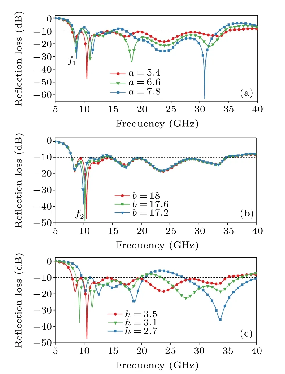
Fig. 4. Reflection loss curves of the PDMA with different dimensional parameters. (a)Arm width of cross-hole a; (b)arm length of cross-hole b; (c)thickness h.
A fabricated PDMA is measured to verify the accuracy of the numerical simulation. As shown in Fig. 5(a), the size of the PDMA sample is 180 mm×180 mm,and is fabricated using a computer numerical control(CNC)engraving machine,supplied by Beijing Jingdiao Group Co.,China. The measurement of the specimen together with an aluminum backplane is performed using an NRL-arch reflectivity test system (a vector network analyzer AV3629 connects two speakers) in an EM microwave chamber. The measured reflection loss in the range of 5 GHz–18 GHz and 26.5 GHz–40 GHz is shown in Fig.6(b),suggesting that the measured results are basically in agreement with the simulated results. However,there are several notable differences between the simulated and measured values,which are believed to be caused by the inevitable deviations of electromagnetic and dimensional parameters.The selected dielectric composite with high permittivity is sensitive to the structural parameters;therefore,a small deviation of the structural parameters may have a great impact on impedance matching and absorbing performance. The measured sample has a larger sized cross-hole due to warping of the sample after processing. Therefore, the measured resonant frequency points in the X band move towards higher frequency,which is consistent with the effects of the dimensional parameters on reflectivity analyzed above. For the same reason, the waveguide samples,which are used to measure electromagnetic parameters, are inevitable machining errors, especially for the samples in the range of the high-frequency Ku and Ka bands.There are deviations between the measured and the simulated values, where the measured reflection loss in the Ku band is smaller than the simulated result but the measured reflection loss in the Ka band is stronger than the simulated one.

Fig.5. (a)The specimen of the fabricated PDMA.(b)The measured reflection loss of PDMA.
4. Conclusion
In this work, a thin broadband PDMA based on a crosshole array was designed and studied. The simulated results illustrate that the presented PDMA achieves a reflectivity level of less than-10 dB from 7.93 GHz–35.76 GHz with a thickness of 3.5 mm. The measured results exhibit similar absorption properties. Two mechanisms that include polarization relaxation of the dielectric and edge effects of the crosshole array are used to study the origin of power loss and the related absorbing performance. The equivalent electromagnetic parameter of the PDMA with high permittivity can be optimized easily by changing structural parameters to achieve wide impedance matching. To some extent, this work overcomes the shortcomings of the narrow absorbing bandwidth of dielectrics. It demonstrates that the PDMA with high permittivity has great potential in the fields of radar stealth and electromagnetic shielding.Acknowledgments
Project supported in part by the Young Scientific and Technological Innovation Talents in Hunan, China (Grant No. 2021RC3003), the Science and Technology Plan Project of Hunan Province, China (Grant No. 2015TP1007), Initial Research Funding for Special Associate Professor by Central South University (Grant No. 202045002), and the National Natural Science Foundation for Young Scientists of China(Grant No.51802353).

- Chinese Physics B的其它文章
- A design of resonant cavity with an improved coupling-adjusting mechanism for the W-band EPR spectrometer
- Photoreflectance system based on vacuum ultraviolet laser at 177.3 nm
- Topological photonic states in gyromagnetic photonic crystals:Physics,properties,and applications
- Structure of continuous matrix product operator for transverse field Ising model: An analytic and numerical study
- Riemann–Hilbert approach and N double-pole solutions for a nonlinear Schr¨odinger-type equation
- Diffusion dynamics in branched spherical structure