
Strain-modulated anisotropic Andreev reflection in a graphene-based superconducting junction
2022-11-21 09:30XingfeiZhou周兴飞ZimingXu许子铭DeliangCao曹德亮andFenghuaQi戚凤华
Chinese Physics B 2022年11期
Xingfei Zhou(周兴飞) Ziming Xu(许子铭) Deliang Cao(曹德亮) and Fenghua Qi(戚凤华)
1New Energy Technology Engineering Laboratory of Jiangsu Province,School of Science,Nanjing University of Posts and Telecommunications,Nanjing 210023,China
2School of Electronic Engineering,Nanjing Xiaozhuang University,Nanjing 211171,China
We investigate the Andreev reflection across a uniaxial strained graphene-based superconducting junction. Compared with pristine graphene-based superconducting junction, three opposite properties are found. Firstly, in the regime of the interband conversion of electron–hole, the Andreev retro-reflection happens. Secondly, in the regime of the intraband conversion of electron–hole, the specular Andreev reflection happens. Thirdly, the perfect Andreev reflection, electron–hole conversion with unit efficiency, happens at a nonzero incident angle of electron. These three exotic properties arise from the strain-induced anisotropic band structure of graphene,which breaks up the original relation between the direction of velocity of particle and the direction of the corresponding wavevector.Our finding gives an insight into the understanding of Andreev reflection and provides an alternative method to modulate the Andreev reflection.
Keywords: graphene,uniaxial strain,anisotropic Andreev reflection
1. Introduction
Graphene, a single atomic plane of graphite with a twodimensional honeycomb lattice,[1]provides a highly practical and prospective platform for studying basic physics and applied physics, such as half-integer quantum Hall effect,[2]Klein tunneling,[3]specular Andreev reflection,[4]topological phase transition,[5–8]superconductivity,[9–12]next-generation electronics and photonics,[13,14]and heterostructure.[15]In the first Brillouin zone, there are two inequivalent cornersKandK′,around which is a conical band structure described by the massless Dirac equation. When a uniaxial strain is applied in graphene, the tilted Dirac cone is found,[16,17]which leads to the same structure of relativistic Landau levels as in pristine graphene,but with a renormalized effective Fermi velocity. In this work, we will show that the uniaxial strain can induce anisotropic and interesting Andreev reflection.
In a normal metal–superconductor(s-wave pairing)junction, when an electron from normal region hits the interface of junction, a hole is reflected to the normal region and a pair of electron coupling a Cooper pair is injected into the swave pairing superconductor,known as Andreev reflection.[18]Owing to the same path of incident electron and reflected hole in the same band(intraband conversion of electron–hole),this process is also called Andreev retro-reflection (ARR).However, the specular Andreev reflection (SAR) was found in a graphene-based superconducting junction,[4]where electron and hole belong to different bands (interband conversion of electron–hole) and then the paths of electron and hole are specular. After that, Andreev reflection is widely studied in many Dirac materials and a general view of intraband (interband) conversion-induced ARR (SAR) is left gradually.[19–35]Whereas,an opposite view,i.e.,interband(intraband) conversion-induced ARR (SAR), was shown in the two-dimensional electron gas system with Rashba spin–orbit coupling,[36]the 8-Pmmnborophene (borophane)-based superconducting junction,[37–39]and the tilted Weyl semimetal hybrid junction.[40]Although only the intraband (interband)conversion-induced ARR (SAR) is believed to happen in graphene previously, in this work, we will show that the interband (intraband) conversion-induced ARR (SAR) can also happen in graphene by applying a uniaxial strain. Besides,we will show that the perfect Andreev reflection, electron–hole conversion with unit efficiency, exists at a nonzero incident angle in graphene, which breaks the previous view that the perfect Andreev reflection only happens at normal incidence in graphene.
The paper is organized as follows. We firstly give the model and basic formalism. Then, the numerical results and theoretical analysis are presented and discussed. Finally, the main results of this work are summarized.
2. Models and methods


Fig. 1. (a) Schematic diagrams for strained graphene-based superconducting junction. The direction of junction is characterized by θ. The bonds parallel to the deformation axis are modified. The pristine (deformed) lattice distance is denoted by a (a′). t (tnnn) represents the nearest neighbor(next-nearest neighbor)hopping amplitude without deformation. t′ (t′nnn) is the hopping amplitude between nearest neighbor (next-nearest neighbor) carbon atoms separated by the deformed lattice distance a′. Schematic diagrams for SAR and ARR through the equal energy surfaces of electron and hole with (b) EF =0 or (c)EF =Δ0 =10 meV and θ =π/4. The black dotted line denotes the conservation of transverse wave vector ky′ in the process of transmission. The incident electron comes from D valley and the reflected hole returns to D′ valley. The direction of wavevector is different from the direction of velocity due to the anisotropic band structure of strained graphene,which makes interband-induced ARR and intraband-induced SAR possible.
According to Fig. 1(a), the relation of the wavevector components in coordinate systemsx–yandx′–y′meets[30,41]

Here the direction ofx′-axis is perpendicular to the interface of superconducting junction, as shown in Fig. 1(a).θis the angle betweenx-axis andx′-axis. By substituting Eq.(4)into Eq. (2), the excited spectrum of electron and hole in the normal region in coordinate systemx′–y′can be obtained. The schematic diagrams for SAR and ARR through the equal energy surfaces of electron and hole withEF=0(EF=Δ0)andθ=π/4 are drawn in Fig.1(b)(Fig.1(c)). Generally,the direction of velocity parallels the direction of wavevector when the band structure is isotropic.But,the direction of wavevector is different from the direction of velocity due to the anisotropic band structure of strained graphene, which makes interbandinduced ARR and intraband-induced SAR possible.
In the coordinate systemx′–y′,owing to the continuity of wavefunctions,the wavefunctions at the interface of NS junction meet


3. Results and discussion
3.1. Anisotropic Andreev reflection


Fig.2. (a)–(d)The incident angle of electron-dependent reflected angle of hole in the different directions of junction. The black (red dashed)line denotes the electron from D(D′)valley while the hole back to D′(D)valley. Here Δ0=10 meV,ε =0.6Δ0,and EF=0.
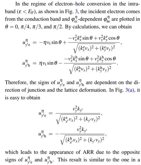


Fig.3. (a)–(d)The incident angle of electron-dependent reflected angle of hole in the different directions of junction. The black (red dashed)line denotes the electron from D (D′) valley while the hole back to D′(D)valley. Here ε =0.6Δ0 and EF=Δ0.
Generally, in a pristine graphene-based superconducting junction, the ARR (SAR) only appears in the regime of the intraband (interband) conversion of electron–hole. But, in a strain-modulated graphene-based superconducting junction,the ARR (SAR) can appear in the regime of the interband(intraband) conversion of electron–hole. The strain-induced anisotropic band structure of graphene, which breaks up the original relation between direction of velocity of particle and direction of the corresponding wavevector,leads to these two anomalous phenomena. In fact,the value of energy-gap functionΔ0does not affect these two anomalous phenomena,i.e.,interband-induced ARR and intraband-induced SAR. On the contrary,these two anomalous phenomena are affected by the tensile strain deeply. In Figs. 4(a) and 4(b), the numerical calculations show that the interband-induced ARR and the intraband-induced SAR are not nearly modulated by energygap functionΔ0. But, in Figs.4(c)and 4(d), it is easy to find that the largerζis, the more obvious these two anomalous phenomena are.
Fig.4. The incident angle of electron-dependent reflected angle of hole in the different values of Δ0 for ε =0.6Δ0, ζ =10%, θ =π/4, and(a) EF =0 or (b) EF =Δ0. The incident angle of electron-dependent reflected angle of hole in the different values of ζ for ε = 0.6Δ0,Δ0=10 meV,θ=π/4,and(c)EF=0 or(d)EF=Δ0.Here the electron comes from D valley while the hole goes back to D′ valley.
3.2. Perfect Andreev reflection


In Fig.5,incident angle-dependentRηandRaηare plotted inEF=0 andθ=0,π/4,π/3, andπ/2. The incident angles of perfect Andreev reflection by numerical calculations is equal to the ones by solving Eq.(9).In Fig.6 withEF=Δ0,the incident angles of perfect Andreev reflection are not changed,which means the perfect Andreev reflection is independent on Fermi energy. In Fig. 7, we give incident angles of perfect Andreev reflection in different directions of junction, where the incident angles is dependent on the conversion order of valley due to the strain-induced anisotropic band structure of graphene.

Fig.5. (a)–(d)The reflected probabilities of electron and hole(Rη and Raη) vs. the incident angle in different directions of junction. Here ε =0.6Δ0,U0=15Δ0,and EF=0.

Fig.6. (a)–(d)The reflected probabilities of electron and hole(Rη and Raη) vs. the incident angle in different directions of junction. Here ε =0.6Δ0,U0=15Δ0,and EF=Δ0.
Fig. 7. Valley-dependent incident angle of perfect Andreev reflectionvs. the direction of junction θ for perfect Andreev reflection.
4. Conclusion
In conclusion, we discuss the Andreev reflection across a uniaxial strained graphene-based superconducting junction.The band structure of graphene becomes anisotropic by applying a uniaxial strain,which induces three interesting phenomena: The Andreev retroreflection happens in the case of interband conversion of electron–hole,the intraband conversion of electron–hole results in the specular Andreev reflection, and the perfect Andreev reflection happens at a nonzero incident angle of electron. Our work provides an alternative and flexible method to tune Andreev reflection.
Acknowledgements
Project supported by the National Natural Science Foundation of China (Grant Nos. 12104232, 11805103, and 11804167), the Natural Science Foundation of Jiangsu Province,China(Grant Nos.BK20190137 and BK20180739),the Innovation Research Project of Jiangsu Province,China (Grant No. CZ0070619002), and NJUPT-SF (Grant No.NY218128).

- Chinese Physics B的其它文章
- A design of resonant cavity with an improved coupling-adjusting mechanism for the W-band EPR spectrometer
- Photoreflectance system based on vacuum ultraviolet laser at 177.3 nm
- Topological photonic states in gyromagnetic photonic crystals:Physics,properties,and applications
- Structure of continuous matrix product operator for transverse field Ising model: An analytic and numerical study
- Riemann–Hilbert approach and N double-pole solutions for a nonlinear Schr¨odinger-type equation
- Diffusion dynamics in branched spherical structure