
Coupling characteristics of laterally coupled gratings with slots
2022-11-21 09:29KunTian田锟YonggangZou邹永刚LinlinShi石琳琳HeZhang张贺YingtianXu徐英添
Chinese Physics B 2022年11期
关键词:唐慧
Kun Tian(田锟), Yonggang Zou(邹永刚), Linlin Shi(石琳琳), He Zhang(张贺), Yingtian Xu(徐英添),
Jie Fan(范杰), Hui Tang(唐慧), and Xiaohui Ma(马晓辉)
State Key Laboratory on High Power Semiconductor Lasers,Changchun University of Science and Technology,Changchun 130022,China
Laterally-coupled ridge-waveguide distributed feedback lasers fabricated without epitaxial regrowth steps have the advantages of process simplification and low cost. We present a laterally coupled grating with slots. The slots etched between the ridge and grating area are designed to suppress the lateral diffusion of carriers and to reduce the influence of the aspect-ratio-dependent-etching effect on the grating morphology in the etching process. Moreover,the grating height in this structure can be decreased to lower the aspect ratio significantly,which is advantageous over the conventional laterally coupled ridge waveguide gratings. The effects of five main structural parameters on the coupling characteristics of gratings are studied by MODE Solutions. It is found that varying the lateral width of the grating can be used as an effective way to tune the coupling strength;narrow slots(100 nm and 300 nm)and wide ridge(2 μm–4 μm)promote the stability of grating coupling coefficient and device performance. It is important to note that the grating bottom should be fabricated precisely.The comparative study of carrier distribution and mode field distribution shows that the introduction of narrow slots can strengthen the competitive advantage and stability of the fundamental mode.
Keywords: Bragg gratings,distributed feedback(DFB)lasers,coupling coefficient,mode field distribution
1. Introduction
In single mode semiconductor lasers and integrated optical devices, Bragg grating as an important and indispensable functional element influences device stability and performance directly. The grating is a wavelength selection element that is made in or near the waveguide of the epitaxial structure to strengthen its interaction with the optical field to realize appropriate distributed feedback in the traditional distributed feedback(DFB)lasers.[1]However,the fabrication of devices with buried heterostructure gratings[2]often requires at least one epitaxial regrowth step after grating definition, which increases the processing complexity and cost. And,the interface defects introduced in the process of epitaxial overgrowth impact the performance and yield of the device.
Laterally-coupled ridge-waveguide (LC-RWG) DFB lasers[3–6]circumvent the above problems. Lateral gratings used in this kind of device can be directly etched on the surface of epitaxial wafer,which significantly simplifies the fabrication process and improves the stability and reliability of the device. However,it is worth noting that this structure has two particularities. Firstly,compared with the buried grating having the same period and duty cycle, surface gratings always require a larger etching depth to increase the overlap between the grating and the optical field,so as to obtain sufficient coupling coefficient. Secondly,after grating fabrication,the grating grooves should be filled with insulating medium to eliminate the influence of impurities and electrode metal on grating grooves.
This device also has its inadequacies. For example,the imperfect morphology of grating grooves caused by the aspect-ratio-dependent-etching (ARDE) effect in the etching process seriously affects the coupling coefficient. There is no doubt that increasing the lateral size of the grating can compensate for the reduction of coupling coefficient at a certain extent. But it brings an extra problem, that is the increased lateral diffusion of pump current. In addition, the uncontrollability of the imperfect profile also adds the complexity of device design and fabrication. Some research results[7–9]indicate that accurate adjustment and control of the coupling coefficient is essential for the design and analysis of DFB lasers.At present, however, there are still no reliable and effective schemes to solve these problems.
Aiming to deal with the problems mentioned above, we proposed a LC grating structure with narrow slots. Introducing a slot between the grating and the non-etched ridge region help to lower the difficulty of making standard grating profile and to achieve a precise fabrication. It also frames a limitation on the lateral spreading of carriers and reduces the interaction between the carrier and the grating.
The paper is organized as follows.The structure proposed and epitaxial layers structure used for modelling are presented in Section 2. The dependence of coupling coefficient and effective refractive index on structural parameters as well as the distributions of carriers and optical field are discussed in Section 3. Theoretical research of coupling coefficient dependence on structural variations is carried out to guide the optimal design of the device. The conclusions are summarized in Section 4. The results indicate that such a structure is beneficial to improve up-to-standard rate of grating profile and yield of devices.
2. Structures for modelling and analysis
The LC DFB structure is based on the conventional LCRWG DFB structure and improved, as shown in Fig. 1. The introduced deep and narrow slots are set between the grating and the non-etched ridge region,and the bottom of slots levels with that of grating grooves. And,the lower height of gratings reduces the grating aspect ratio.
The manufacturing process of this structure can be as follows: the first lithography and etching are used to form ridge;then,gratings and slots on the both sides of ridge are fabricated in the second lithography and etching and,in lateral direction the epitaxial layers outside the grating area are removed; after dielectric film deposition on the top of wafer, the p electrode window is opened in the third lithography and etching.It should be noted that to reduce the impact of ARDE effect on the slot structure in the etching process,some distances are set between the side wall of the ridge formed in the first etching and the slot.

Fig.1. Schematic 3D views of LC DFB structure with slots.

Fig.2. The epitaxial growth structure.
The vertical structure of wafer used in the simulation and analysis is shown schematically in Fig. 2. A straincompensated InGaAs/GaAs/GaAsP single quantum well active region is applied to realize the emission wavelength about 1.06 μm,And,asymmetric AlGaAs confinement and cladding layers are adopted to reduce the absorption loss of device and increase the optical confinement factor difference between the fundamental mode and higher-order modes, so as to realize the efficient and stable operation of device. The implemented LC grating is 1st order, which leads to a period of 0.16 μm,according to the Bragg condition(λBragg=1.064 μm).
3. Simulation and analysis
3.1. Modeling and structural parameters
Figure 3 plots a cross-sectional view of the device(without electrodes). An important issue for the DFB laser diodes and integrated photonics devices is the sensitivity of structural characteristics to dimensional variations.Some structural changes caused by the process can affect the field distribution and carrier distribution of the device to varying degrees, so these influences need to be clarified. Five parameters were studied: narrow ridge widthWn, wide ridge widthWw, slot widthWs,grating widthWgand variation of grating height ΔH.In the simulation and analysis process,the structure is simplified,the cap layers and electrodes are removed due to the fact that they have little effect on the grating coupling coefficientκand the effective refractive indexneff. The initial value ofWwis set to 2 μm, and the grating widthWgis 2.5 μm. The total lateral width of the structure is 15 μm.The area outside p electrode window is covered with silica. The grating period and duty cycle are 0.16 μm and 0.5,respectively. The distance between the grating top and the ridge top isHr-Hg=0.655 μm.TheκLof device studied in this paper is set to 1.25. For a typical 500 μm cavity length,κof the LC grating is 25 cm-1,thus, the reflectivity of the corresponding passive grating is 0.71858. The structure is modeled by MODE Solution. A TE polarization fundamental mode source is used for calculations. The longitudinal grid length is 0.02 μm,and the lateral and transverse grids are 0.025 μm.
As slot is the key structure in the device and interacts with the optical mode, three structures with different slot sizes are optimized for comparison to identify and evaluate their influence onκ.[10]Theκof proposed structures(A,B,and C)and traditional LC-RWG DFB structure(D)are set near 25 cm-1as shown in Table 1. In addition to the parameters in the table, the initial values of other structural parameters of three structures are the same.
The data comparison from the table shows that as the slot widthWsincreases,the grating depthHgneeds to be added to obtain the targetκ,which could be expected,since the widening of slot reduces the overlap between the grating and the optical field. In addition,it is clear that the grating aspect ratio of the structure (A, B, and C) is less than half of aspect ratio of D,which can help drop the processing difficulty of gratings and slots greatly.

Table 1. Four structures for comparative analysis.
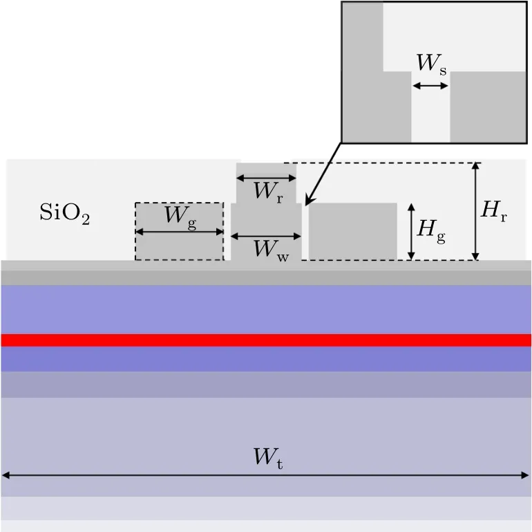
Fig.3. Cross section of the structure used in simulation.
3.2. Ridge width
The dependence ofκandneffonWnis illustrated in Fig.4.With the decline ofWnfrom 2 μm to 1 μm,κof three structures increase slightly. This is because the decrease ofWnenhances the transverse confinement of ridge on the optical mode,making more optical field enter the grating area. What is more,the data comparison between three structures demonstrates that larger slot gives rise to higher sensitivity ofκtoWnvariations. In addition, the variation ofWnhas little effect onneffof waveguide,which is due to the fact that the optical field decays rapidly in the ridge and the intensity of the field near the narrow ridge is very weak. Considering that the influence of a small reduction ofWnon theκandneffcan be ignored and the decrease ofWnwill help weaken the influence of ARDE effect on slot morphology during etching,Ww-Wn=0.2 μm is set as a fixed relationship in the subsequent simulation and analysis.
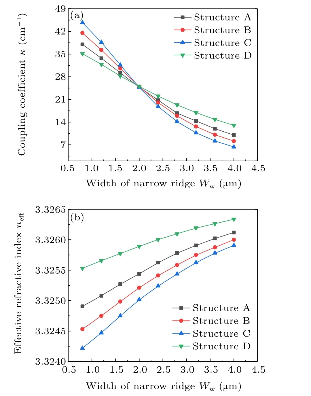
Fig.5. The dependence of(a)κ and(b)neff on Ww.
Figures 5(a) and 5(b) depict theκandneffas functions ofWwrespectively. Obviously,κdecreases asWwincreases,which can be attributed to the fact that the increase ofWwmakes the mode more confined in the ridge,reducing the overlap between the grating and the optical field. Furthermore,with the decline ofWw,the growth ofκaccelerates gradually,which means that smallWw(<1.5 μm)is not suitable for the device due to the high sensitivity ofκtoWwvariations. It is important to know that from practical aspect, too narrow a ridge results in the increase of electrical resistance and lithography alignment difficulty of electrode window. A ridge width of 2 μm–4 μm is recommended. In addition, it can be found that the larger the slots is, the higher the slope ofκbecomes and, asWwincreases, theneffof waveguide keeps improving.This shows that too wide slot will increase the sensitivity ofκtoWwvariations,so it is not suitable for device structures.
3.3. Grating width
Forκandneffdependence on the lateral width of grating,Wgis increased from 1.5 μm to 3.5 μm and other parameters are kept. Figure 6(a)indicates that the grating width variation influencesκevidently. The reason is that the increase ofWgpulls more optical field into the grating region and expands grating confinement factor,which is accepted and foreseeable.The comparison of the four structures shows that for the structures with wider slots,κchanges more rapid withWg. In this case,the grating with narrow slots is conducive to theκstability of the device. In addition,it can be seen from Fig.6(b)that the change ofWgwill not exert a significant effect on waveguideneff. These characteristics enable that broadening the lateral width of grating is an effective way to realize the accurate adjustment ofκ.

Fig.6. The dependence of(a)κ and(b)neff on Wg.
3.4. Grating height
The deviation of grating top and bottom from the design position caused by process error affectsκandneff.Their influence effect and law are of great importance and have reference value for the adjustment of device parameters and process conditions.
When ΔHis less than 0,the grating is overetched;otherwise the grating is not etched enough. As can be seen from Fig.7(a),with the rise of grating top,κincreases slightly,and the growth rates of three structures are very close. This is because the expansion of transverse size of the grating improves its overlaps with the optical field. However, for grating bottom,a small change of position can cause obvious variation ofκ. The comparison shows that the position change of grating bottom is more likely to influenceκandneff. Theκchanging rates as a function of ΔHare 9.426×104cm-2(grating top)and 1.46×106cm-2(grating bottom). The reason for the difference is that the intensity of optical field near the bottom of gratings is higher than that near the top. This also means that the position of the grating bottom needs to be precisely etched, and a priority should be given to the introduction of etching stop layer.
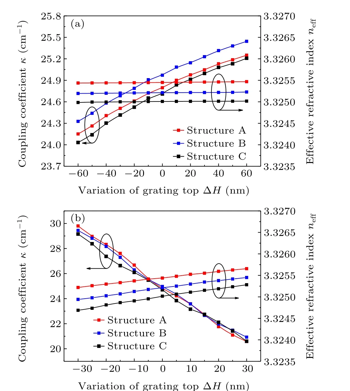
Fig.7. The κ and neff versus variation of grating top(a)and bottom(b).
3.5. Distributions of carriers and optical field
In traditional LC-RWG DFB lasers,during the downward transmission of the current in the ridge, some carriers will spread into the lateral grating,reducing the injection efficiency of the device.Separating the grating and the ridge is a straightforward way to hinder carrier lateral diffusion.
The left panel of Fig. 8 shows the carrier distribution of semi structure of LC DFB lasers with slots and conventional LC-RWG DFB lasers. The carrier distribution of four structures is calculated by Crosslight PICS3D.The right panel of Fig. 8 shows the optical field distributions of fundamental mode, first- and second-order mode (λBragg=1.064 μm)simulated by MODE Solutions. While multiple lateral optical modes supported in waveguide structures are not desired,they are for comparison only.
By comparing the four figures on the left panel, we can find that the carrier distribution of LC DFB lasers with slots is distinctly different from that of conventional LC-RWG DFB lasers. In structure D, the lateral spreading of carriers into grating region is obvious. What is more,there appears the aggregation of carriers at the lateral edge of the grating region and near the bottom of the p-cladding,the optical field intensity of the fundamental mode is weak here,which is opposite to that of the first and second-order modes. The coupling between carriers with high order modes in this region decreases the lateral mode discrimination.However,the incorporation of slots effectively restricts the lateral spreading of carriers and weakens carrier aggregation,allowing for a better carrier confinement.

Fig.8. Carrier distribution of four lasers(left panel). (a)Semi structure of A.(b)Semi structure of B.(c)Semi structure of C.(d)Semi structure of D.Optical field distribution of fundamental mode,first-order mode and second-order mode(right panel),The first column shows fundamental mode,the second shows first-order mode and the third shows second-order mode. In the figure,the carrier distribution and three field distributions in a row belong to the same device.
It can be seen from the graphs of right panel that the change of slot structure has an substantial effect on the field distribution. Enlargement of slots dimensions increases the confinement of the waveguide structure on the optical mode in transverse direction. Moreover, the growth of slot size increases the distance between the two intensity centers of the first-order mode field,raising the threshold gain of first order mode. For second order mode,there is a considerable overlap between the optical field and the ridge,which helps to obtain sufficient gain. However, the field intensity in the side grating reduces as the increase of slot size, resulting in insufficient coupling. In summary, compared with the fundamental mode,higher-order modes have similar overlap with the active region, but lowered mode gain or insufficient wavelength selectivity,which helps to strengthen the competitive advantage of the fundamental mode and the mode stability of the device.
4. Conclusion
We have put forward a laterally-coupled grating with slots set between the ridge and grating region. Such a structure not only restricts the lateral current leakage but also reduces the impact of ARDE effect on grating profile. In addition,compared with the traditional LC-RWG grating structure,this structure has a decreased grating height, which significantly reduces the difficulty of grating etching. Simulation results show that the lateral width of gratings as an important parameter can be altered to tailor the coupling coefficient. Moreover,it is also found that narrow slots (100 nm and 300 nm) and wide ridge(2 μm–4 μm)contribute to the stability of grating characteristic and device performance. It should be noted that grating bottom needs to be precisely fabricated to ensure the accuracy ofκ. The comparative analysis of carrier distribution and multi-mode field distribution shows that the addition of narrow slots can enhance the competitive advantage and the stability of fundamental mode.
Acknowledgments
Project supported by the National Natural Science Foundation of China (Grant Nos. 61804013, 61804014, and 61805023) and Department of Science and Technology of Jilin Province, China (Grant Nos. 20190302052GX and 20210201030GX).
猜你喜欢
数学小灵通(1-2年级)(2022年11期)2022-11-21
数学小灵通(1-2年级)(2022年11期)2022-11-21
数学小灵通(1-2年级)(2022年11期)2022-11-21
数学小灵通(1-2年级)(2022年6期)2022-06-17
数学小灵通(1-2年级)(2022年6期)2022-06-17
数学小灵通(1-2年级)(2022年5期)2022-06-01
数学小灵通·3-4年级(2022年3期)2022-03-17
数学小灵通(1-2年级)(2022年3期)2022-03-17
读写算·小学中年级版(2016年5期)2016-05-14
读写算·小学低年级(2016年9期)2016-05-14

- Chinese Physics B的其它文章
- A design of resonant cavity with an improved coupling-adjusting mechanism for the W-band EPR spectrometer
- Photoreflectance system based on vacuum ultraviolet laser at 177.3 nm
- Topological photonic states in gyromagnetic photonic crystals:Physics,properties,and applications
- Structure of continuous matrix product operator for transverse field Ising model: An analytic and numerical study
- Riemann–Hilbert approach and N double-pole solutions for a nonlinear Schr¨odinger-type equation
- Diffusion dynamics in branched spherical structure