
Ultra-wideband surface plasmonic bandpass filter with extremely wide upper-band rejection
2022-11-21 09:28XueWeiZhang张雪伟ShaoBinLiu刘少斌QiMingYu余奇明LingLingWang王玲玲KunLiao廖昆andJianLou娄健
Chinese Physics B 2022年11期
Xue-Wei Zhang(张雪伟), Shao-Bin Liu(刘少斌), Qi-Ming Yu(余奇明),Ling-Ling Wang(王玲玲), Kun Liao(廖昆), and Jian Lou(娄健)
College of Electronic and Information Engineering,Key Laboratory of Radar Imaging and Microwave Photonics,Ministry of Education,Nanjing University of Aeronautics and Astronautics,Nanjing 211106,China
An ultra-wideband bandpass filter(BPF)with a wide out-of-band rejection based on a surface plasmonic waveguide(SPW)slotline with ring grooves is designed and analyzed. A paired microstrip-to-slotline transition is designed for quasi-TEM to TM mode conversion by using a microstrip line with a circular pad and the slotline with the same circular slot. The mode conversion between the TM and the surface plasmon polariton (SPP) mode is realized by using a gradient slotline with ring grooves and an impedance matching technique. The upper cut-off frequencies of the passband can be adjusted by using these proposed SPP units, while the lower frequencies of the passband are created by using the microstrip-toslotline transitions to give an ultra-wideband BPF. The dispersion curves of SPP units, electric field distribution, and the transmission spectra of the proposed ultra-wideband bandpass filter are all calculated and analyzed by the finite-difference time-domain(FDTD)method. The simulated results show that the presented filter has good performance including a wide 3-dB bandwidth of 149% from 0.57 GHz to 3.93 GHz, an extremely wide 40-dB upper-band rejection from 4.2 GHz to 18.5 GHz,and low loss and high selectivity in the passband. To prove the design validity,a prototype of the BPF has been manufactured and measured,showing a reasonable agreement with simulation results. The unique features of the proposed BPF may make it applicable for integrated circuit and plasmonic devices in microwave or THz frequency ranges.
Keywords: surface plasmonic waveguide(SPW),bandpass filter,out-of-band rejection,ultra-wideband
1. Introduction
Surface plasmon polaritons(SPPs)are a kind of electron density wave formed by the interaction between electromagnetic wave and free charge on the metal surface.[1]The unique transmission characteristics of an SPP make it rapidly applied in the optical band.[2,3]In 2004, Pendryet al. demonstrated slow-wave transmission in microwave segment by etching air slots periodically arranged at a sub-wavelength spacing in a metal cube to simulate the dispersion characteristics of SPPs in the microwave or millimeter-wave band.[4]This structure is called spoof surface plasmon polaritons (SSPPs), which simulates the transmission characteristics of natural SPPs through artificial periodic arrays.[5]To date, a variety of different SSPP structures have been proposed,with operating frequencies that cover the microwave,millimeter-wave,and terahertz band.[5–9]However, all the previous work has been to guide SSPP propagation through a three-dimensional(3D)structure,which cannot meet the requirements of miniaturization and high integration of modern communication systems.
In 2013, Cuiet al. first proposed the realization of planar SSPPs using an ultra-thin surface plasmonic waveguide(SPW) with approximately zero thickness.[10]In 2014, a matching transition was proposed for conversion between the quasi-TEM waves and the surface plasmons.[11]Since then,the planar SPW represented by this corrugated metal strip structure has been studied extensively and applied in a variety of microwave circuits.[12–16]It is well known that the dispersion of SSPPs shows wide low-pass frequency characteristics,and the steep cut-off sideband of the SSPP filter also shows a low-pass band.[4,5,10]Therefore, the direct application of the SPW in the microwave band is to realize a low-pass filter,because its cut-off sideband is much steeper than a conventional filter.[17–20]However,when SSPP is used to implement the filter, it shows a large reflection coefficient and insertion loss in the low-frequency band close to zero Hz.[21–23]Hence, to realize the SPW BPF, it is only necessary to introduce lowfrequency transmission zeros to suppress the lower frequency band. Researchers have constructed ultra-wideband bandpass filters with good performances in various ways,[14–23]but the out-of-band suppression characteristic of the BPF is infrequently considered.
The ultra-wideband surface plasmonic filter has the advantages of low insertion loss, convenient manufacture, wide bandwidth,and flexible integration with other circuits,so it is considered to be the development direction for next-generation communication systems. Thus, some efforts have been made in the design of UWB filters,such as the slow-wave half-mode SIW,[14]ultra-thin symmetric SPW,[15–20]and hybrid SSPP and SIW,[24]but their effectiveness on upper-band rejection and sideband selectivity is still limited.
In this paper,the novel slotline SSPP bandpass filter with ultra-wide passband and wide upper stopband is proposed. It consists of a top microstrip feed layer and a bottom plasmonic slot waveguide with a ring grooves layer. The dispersion and transmission characteristics of the slot waveguide with ring grooves are investigated, followed by the design and analysis of the matching structure between the slot and plasmonic waveguide. The simulated results show that the proposed bandpass filter not only ensures a wide passband,but also has a wide out-of-band suppression characteristic, and the upper and lower cut-off bands are independently adjustable. The experimental results of the fabricated sample agree with the simulation results well, which proves the design validity. This work builds a solid foundation for the advanced plasmonic functional device.
2. Design and analysis
Figure 1 shows the proposed slotline SPW with ring grooves, in which the yellow part is copper and the blue part is dielectric. The unit structure is arranged periodically in thex-direction. The dielectric substrate is the commercially available F4B, whose dielectric constant is 3.5, thickness 0.508 mm, and loss tangent 0.001. The slotline SSPP waveguide is a one-dimensional array of rectangular and ring grooves with widthg, depthh, radiusrof the ring groove,width of the central slotline waveguidew, and period of the unit cellsP,as shown in Fig.1.
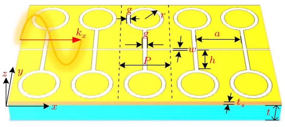
Fig.1. Geometry of the proposed slotline SPW with ring grooves. Reference dimensions are P=5,w=0.17,g=0.4,r=2,h=3,a=4.6,and t=0.508(unit: mm).
It is universally acknowledged that the ultra-thin SPW structures can support fundamental mode and high-order mode transmission. Firstly, to determine the conditions of singlemode transmission, the dispersion characteristics of the proposed SPW structure are numerically calculated and analyzed by the finite-difference time-domain (FDTD) method, which is very important for the design of bandpass filters with wide stopband characteristics. In our analysis, dispersion curves of the proposed SSPP unit cell with different groove depthhare shown in Fig. 2(a). The light line in Fig. 2(a) represents the dispersion curve of electromagnetic waves transmitted in a vacuum. The dispersion curve only appears in the fundamental mode, and the dispersion diagrams of the fundamental mode of the SSPP deviate markedly from the light line (that is, the slow-wave region) whenh <P, as shown in Fig. 2(a). In addition, we can see that the asymptotic frequency for the fundamental mode of the SSPP decreases as the depth of the grooves increases. However, the high-order mode of SSPP units is excited in a certain range of frequencies whenh >P,as shown in Fig.2(a). Therefore,the number of modes in the proposed SPW structure is closely related to the groove depthh, which will excite the higher order modes when the groove depth is greater than the periodic length of the units. The corresponding transmission coefficients(|S21|)of the SPW structure with differenthare depicted in Fig.2(b).It can be observed that with the increase of groove depth,there are multiple passbands in the transmission spectrum, corresponding to each mode of the dispersion curve in Fig. 2(a).We find that only one passband appears in a wide frequency band whenh=3 mm(h <P),corresponding to the characteristics of single-mode transmission,as schematically illustrated in Fig.2(b). Thus,a low-pass filter can be realized by selecting appropriate parameters to make the SPW work in single mode.

Fig.2. (a)Dispersion curve of the proposed SSPP unit cell with different h.(b)The corresponding transmission coefficients(|S21|).
We have designed an ultra-wideband SSPP bandpass filter based on the proposed slotline SPW, which is composed of a microstrip-to-slotline feed structure, transition structure,and slotline SPW with ring grooves structure, as shown in Fig. 3. The detailed region I of Fig. 3 shows the microstrip with circular plate feeding lines and the slotline with the same circular slot, which is used for quasi-TEM to TM mode conversion. The widthwof the slotline waveguide is 0.17 mm.The widthl0and lengthl1of the microstrip lines are 1.1 mm and 11.12 mm,respectively.Region III is the proposed slotline plasmonic waveguide ofN-cascaded SSPP units. As depicted in Fig. 3(b), region IV and region V are mirrored symmetrically with region II and region I along they-direction,respectively.The geometrical dimensions in Fig.3(b)areh1=1 mm,h2= 2 mm,h3= 4 mm,h4= 1.72 mm,h5= 3.14 mm,r1=1.3 mm,r2=1.6 mm,N=3,andr0=R=4 mm.

Fig.3. Two-dimensional(2D)schematic diagram of the proposed ultra-wideband SSPP bandpass filter. (a)The top view. (b)The bottom view.
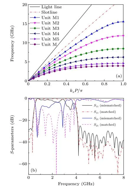
Fig. 4. (a) Dispersion curves of different units in region II of the bandpass filter. (b) The simulated S-parameters of the plasmonic bandpass filter with and without the matching structure.
We notice a significant mismatch of momentum between the slotline that supports TM waves and the proposed SPW that supports the SSPP, as shown in Fig. 4(a). To solve the problem,a matching structure from the slotline to the SPW is designed and demonstrated to make the momentum gradually match between the slotline and plasmonic waveguide as shown in Fig. 4(a). The matching structure is composed of grooves and ring grooves with five different unit sizes based on the wave vector and impedance matching technique, as shown in region II in Fig. 3(b). To demonstrate efficient single-mode transmission,figure 4(b)shows the simulatedS-parameters of the plasmonic bandpass filter with and without the matching structure. The plasmonic bandpass filter without the matching structure will have a large reflection loss and very low transmission efficiency. However, small reflection loss and highefficiency transmission in the passband can be achieved in the proposed BPF by introducing the proposed matching structure,as shown in Fig. 4(b). The high-performance filter passband has a UWB frequency range from 0.57 GHz to 3.93 GHz, in which the reflection coefficient is lower than-11 dB and the average insertion loss is less than 0.5 dB.Therefore,the above results in Fig.4 give a very good insight into the larger propagation loss of the SPW in Fig.2(b)with the black solid line.It can be seen from Fig.4(a)that the more matching structural units, the better the matching effect of wave vectors will be,but the physical size of the filter structure will be increased at the same time. Hence,to miniaturize the overall design of the BPF, we did not use more matching structural units because the proposed matching structure already has a better matching effect.
To verify the high-pass characteristics of the microstripto-slotline feed structure, a high-pass filter based on the microstrip with a circular plate-to-slotline conversion structure was designed,as shown in the inset of Fig.5(a).The high-pass filter consists of two microstrip with a circular plate-to-slotline conversion structures and slotline waveguides with a width ofw. The circular slot line is used as an impedance matching structure at low frequency to improve the impedance matching of the high-pass filter, in which the radius of the circular slot determines the lower cut-off frequency of the high-pass filter.Figure 5(a)shows the simulatedS-parameters of the proposed microstrip-to-slotline transitions structure with different values ofr0. The lower cut-off frequency of the high-pass filter decreases with the increase in the radiusr0of the circular slot,as shown in Fig. 5(a). Figure 5(b) shows the corresponding transmission coefficients of the proposed SSPP BPF varying with the radius of the circular slot. It can be clearly seen from the illustration in Fig.5(b)that the lower cut-off frequency of the BPF decreases with the increase inr0,which is consistent with the change of the transmission spectrum of the high-pass filter in Fig. 5(a). Therefore, the lower cut-off frequency of the BPF can be adjusted within a certain frequency range by adjustingr0.
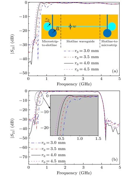
Fig. 5. (a) Simulated S-parameters of the proposed microstrip to slotline transitions with different values of r0. (b) The corresponding transmission coefficients of the proposed SSPP BPF.
To explore the performance of the designed BPF more clearly, we analyze the key geometrical dimensions of the structure. According to the analysis of the transmission characteristics of the SPW proposed in Fig. 2, the groove depthhhas an important influence on the dispersion characteristics. The calculated dispersion curve of the proposed SSPP units with different values ofhunder the guarantee of efficient single-mode transmission is shown in Fig. 6(a). We can see that the asymptotic frequency increases as the groove depth decreases. Figure 6(b) shows the transmission performance of the BPF with varying depthh; obviously, the upper cutoff frequency edge of the transmission spectrum is consistent with the asymptotic frequency of the corresponding dispersion curve. Meanwhile, an extremely wide 40-dB upper-band rejection from 4.2 GHz to 18.5 GHz can be obtained when the grove depthhis 3.0 mm. Therefore, the upper cut-off frequency of the BPF can be adjusted by changing the groove depth of the SSPP units. The above results indicate that the cut-off frequency of the upper and lower sideband of the BPF can be independently controlled by changing the structural parameters of the SPW and microstrip-to-slotline transitions,respectively.

Fig.6.(a)Calculated dispersion curve of the SSPP units with different values of h. (b)The corresponding S-parameters.

Fig. 7. The simulated electric field distribution of the z-component on the x–y plane above the top surface of the filter at (a) 0.4 GHz, (b) 3 GHz, and(c)6 GHz.
To further obtain the SSPP propagation characteristics of the BPF, the simulated electric field distribution of thezcomponent on thex–yplane above the top surface of the filter at 0.4 GHz,3 GHz,and 6 GHz are plotted in Figs.7(a)–7(c),respectively. We find that only the signals at 3 GHz can be propagated through the BPF because the signals are in the designed passband. The signals at 6 GHz vanish rapidly along the SSPP propagation direction because the frequency is above the cut-off frequency of the SSPP unit structure,as illustrated in Fig.7(c). Moreover,owing to the introduction of the structure of the microstrip-to-slotline transitions,the waves cannot be transmitted through the slotline waveguide at 0.4 GHz, as shown in Fig.7(a).
3. Experimental results
In order to verify the correctness of the design method,the designed BPF is produced according to the schematic diagram of Fig.3. A prototype of 113 mm×20 mm is fabricated and measured. Specifically,the metallic pattern is realized by PCB technology on the 0.508 mm thick F4B (εr=3.5) substrate. Figure 8 shows a photograph of the fabricated BPF.The prototype BPF was measured by an Agilent N5245A vector network analyzer.
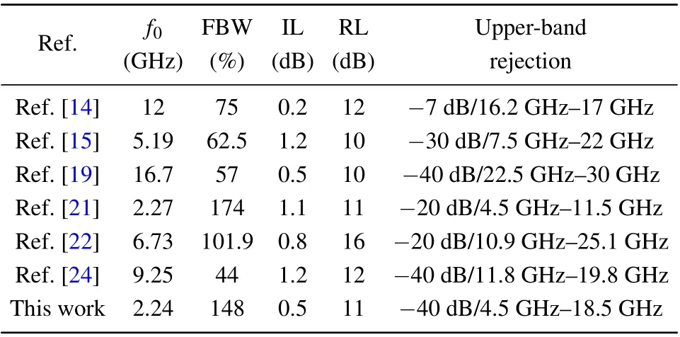
Table 1. Performance comparison.

Fig. 8. Photograph of the fabricated filter. (a) The top view. (b) The bottom view.
As shown in Fig. 9, the measured and simulated results of the proposed BPF are completely consistent,which demonstrates the design’s correctness. In particular,the results show that the 0.5 dB average insertion loss can be achieved from 0.6 GHz to 3.85 GHz, and the 3-dB fractional bandwidth from 0.58 GHz to 3.9 GHz with 148%,as shown in the passband view in Fig. 9(a). Meanwhile, the passband of the filter achieves a high rectangular coefficient, which greatly enhances the reliability of the bandpass filter. Moreover,a wide 40-dB upper-band rejection can be observed from 4.5 GHz to 18.5 GHz, which is a slightly higher|S21| compared to the simulated results,as shown in the wide spectrum range view in Fig.9(b).This discrepancy can be permitted because when the out-of-band transmission is less than-40 dB,the transmission energy of the signal is already very weak,and the measured results are very sensitive to the noise of the equipment.

Fig.9. Measured and simulated S-parameters of the BPF.(a)The passband view. (b)The wide spectrum range view.
A comparison with other related work is shown in Table 1 to verify the good performance of the ultra-wideband SSPP BPF with a wide upper-band rejection,in whichf0,FBW,RL,and IL expresses the central operating frequency, fractional bandwidth, return loss, and insertion loss, respectively. We can see from Table 1 that the proposed BPF has good performance in terms of working bandwidth,low insertion loss,and out-of-band rejection.
4. Conclusion
In this article, an ultra-wideband bandpass filter based on a slotline SPW, which is composed of rectangular groove and ring grooves structures, has been presented. The electric field distribution, dispersion, and transmission characteristics of the proposed SPW structure are analyzed. The mode conversion of quasi-TEM to TM mode and TM to the SPP mode of the proposed matching structure is applied to design the UWB filter. Moreover, the effect of the geometrical parameters of the filter on the transmission characteristics is investigated, in which the upper and lower stopband are independently adjusted. Results indicate that a filter working bandwidth with 0.5 dB insertion loss can be achieved from 0.57 GHz to 3.39 GHz with an extremely wide 40-dB upperband rejection from 4.2 GHz to 18.5 GHz. A prototype of the proposed BPF has been manufactured and measured,measurement and simulation results show good agreement. This work can be used in the design of suppressing wide out-ofband noise signals and broadband microwave filters.
Acknowledgments
Project supported by the National Natural Science Foundation of China (Grant Nos. U2141232, 62071221, and 62071442)and the Aeronautical Science Foundation of China(Grant No.2019ZA037001).

- Chinese Physics B的其它文章
- A design of resonant cavity with an improved coupling-adjusting mechanism for the W-band EPR spectrometer
- Photoreflectance system based on vacuum ultraviolet laser at 177.3 nm
- Topological photonic states in gyromagnetic photonic crystals:Physics,properties,and applications
- Structure of continuous matrix product operator for transverse field Ising model: An analytic and numerical study
- Riemann–Hilbert approach and N double-pole solutions for a nonlinear Schr¨odinger-type equation
- Diffusion dynamics in branched spherical structure