
Experimental demonstration of a fast calibration method for integrated photonic circuits with cascaded phase shifters
2022-11-21 09:35JunqinCao曹君勤ZhixinChen陈志歆YaxinWang王亚新TianfengFeng冯田峰ZhihaoLi李志浩ZeyuXing邢泽宇HuashanLi李华山andXiaoqiZhou周晓祺
Chinese Physics B 2022年11期
关键词:华山
Junqin Cao(曹君勤), Zhixin Chen(陈志歆), Yaxin Wang(王亚新), Tianfeng Feng(冯田峰),Zhihao Li(李志浩), Zeyu Xing(邢泽宇), Huashan Li(李华山), and Xiaoqi Zhou(周晓祺)
School of Physics and State Key Laboratory of Optoelectronic Materials and Technologies,Sun Yat-sen University,Guangzhou 510000,China
With the development of research on integrated photonic quantum information processing,the integration level of the integrated quantum photonic circuits has been increasing continuously, which makes the calibration of the phase shifters on the chip increasingly difficult. For the calibration of multiple cascaded phase shifters that is not easy to be decoupled,the resources consumed by conventional brute force methods increase exponentially with the number of phase shifters,making it impossible to calibrate a relatively large number of cascaded phase shifters. In this work, we experimentally validate an efficient method for calibrating cascaded phase shifters that achieves an exponential increase in calibration efficiency compared to the conventional method,thus solving the calibration problem for multiple cascaded phase shifters.Specifically, we experimentally calibrate an integrated quantum photonic circuit with nine cascaded phase shifters and achieve a high-precision calibration with an average fidelity of 99.26%.
Keywords: cascaded phase shifters,calibration,quantum photonic chip
1. Introduction
By exploiting quantum mechanical effects, quantum information technologies promise significant advantages in communication,[1–5]computation,[6–11]and measurement.[12–15]Among various physical systems for quantum information processing, photons have received considerable attention because of their fast propagation speed,easy manipulation and noise immunity. Quantum information research based on optical systems have made great progress[16–31]and have achieved quantum supremacy[32–34]recently. As the complexity of optical quantum information processing tasks increases,the number of optical components required increases dramatically, which leads to a continuous increase in sizes of optical circuits,making it a natural choice to move the entire system to an integrated optical platform.So far, a variety of experiments based on integrated quantum photonic circuits have been reported, including on-chip quantum logic gates,[35]on-chip multi-photon entanglement sources,[36]and experimental demonstrations of on-chip quantum algorithms and quantum simulations.[37]The latest quantum photonic chip have integrated nearly one thousand optical components.[38]
With the increase in the size of a quantum photonic chip,it becomes increasingly difficult to calibrate the large number of phase shifters on the chip, especially for the case of multiple cascaded phase shifters that is not easy to be decoupled. For example, for the quantum photonic chip with more than 70 phase shifters presented in Ref.[39], there are multiple cascaded structures with five phase shifters that are hard to be decoupled. To calibrate these phase shifters,the authors selected 10 voltages for each phase shifter, for a total of 105voltage combinations, and then fitted the sampling points accordingly. This calibration method, in which the number of sampling points increases exponentially with the number of cascaded phase shifters, is time consuming and not scalable.Similarly,for some special quantum information applications,such as blind quantum computing,[40]qubits encoded in two paths need to pass through multiple unitary transformations in succession to accomplish the specified function, and this requires cascading multiple phase shifters on the chip and calibrating these phase shifters. To solve this problem, Xinget al.[41]recently proposed an efficient calibration method that requires the number of sampling points to grow only linearly with the number of cascaded phase shifters.
In this work,we report an experimental demonstration of this efficient calibration method on a photonic chip. Specifically,we experimentally prepare a nine-phase shifter cascaded silicon-based quantum photonic chip and efficiently calibrate all nine phase shifters, achieving a high-precision calibration with an average fidelity of 99.26%. Our experimental results show that the number of sampling points required by using this new method increases only linearly with the number of cascaded phase shifters,achieving an exponential resource saving compared to the conventional calibration method.[39]
2. Methodology
2.1. Calibration of a single phase shifter
Here the phaseθof the phase shifter has the following relationship with the currentIapplied on the phase shifter[42,43]

whereγandφare unknown constant parameters. The socalled calibration of the phase shifter is to confirm the specific values ofγandφ.
To calibrate this phase shifter,we let light input from the upper rail and measure the power output from the upper rail.The output state can be written as

whereηis a constant to be determined relating to the MMI splitting ratio.
By changing the currentIapplied on the phase shifter,the optical path difference between the upper and lower rails can be altered, thus enabling the phase-shifting operation of the path-encoded optical qubit. The matrix form of this phaseshifting operation can be written as

The ratio of the output power to the input power is the transmittanceT,which can be expressed as
whereη,γandφare all constants to be determined. The currentIis varied experimentally and then multiple sets ofTandIvalues are measured. As shown in Fig.1(b),the next step is to fit the data ofTandIusing Eq. (5), and the values ofη,γandφcan be determined,thus completing the calibration of the MMI splitting ratio and the phase shifter simultaneously.

Fig. 1. Schematic diagram of the calibration method for the photonic circuit with cascaded phase shifters. (a) The photonic circuit with a single phase shifter. (b) The variation of the transmittance T with the square of the current applied on the phase shifter. (c) The photonic circuit with cascaded phase shifters. (d)The variation of the range of the transmittance ΔT with the square of the current applied on the nth phase shifter. (e)Equivalent photonic circuit for calibrating the(n-1)th phase shifter. (e)Equivalent photonic circuit for calibrating the(n-2)th phase shifter.
2.2. Calibration of cascaded phase shifters
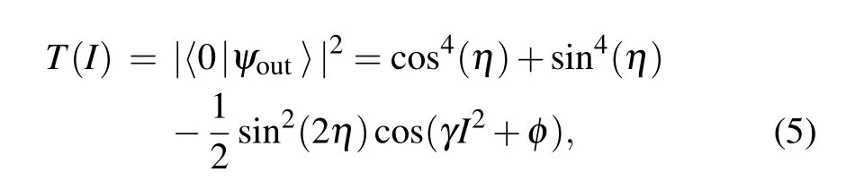
Now let us analyze how to calibrate a circuit with multiple cascaded phase shifters. As shown in Fig. 1(c),nphase shifters are sandwiched betweenn+1 MMIs.We first describe how to calibrate the last phase shifter.


whereα,η,γn, andφnare all constants to be determined.The currentInis varied experimentally, and for eachIn, traverseIn-1to measure the maximum and minimum values of the transmittance and calculate their difference ΔT.
As shown in Fig.1(d),the data of ΔTandInare then fitted using Eq. (9), and the values ofα,η,γn, andφncan be determined, thus completing the calibration of thenth phase shifter.
Calibration of other phase shifters—Let us proceed to calibrate the(n-1)th phase shifter.Since thenth phase shifter has been calibrated,we can setθnto an arbitrary phase. It can be found by calculation that whenθnis set toφ,in which
This means that the last two MMIs together with thenth phase shifter equivalently implement the function of a single MMI(with a fixed additional phase shiftωintroduced before and after the MMI). As shown in Fig. 1(d), the (n-1)th phase shifter thus equivalently becomes the last phase shifter sandwiched between two MMIs and can therefore be calibrated using the method described above to identifyγn-1andφn-1.Note that the final calibratedφn-1has to be subtracted fromωsince a fixed additional phase shiftωis introduced.
Next we calibrate the (n-2)th phase shifter. Similarly,by settingθn=π,we obtain

which means that the last two MMIs are equivalently removed and both thenth and (n-1)th phase shifters no longer have an effect on the transmittanceT. As shown in Fig. 1(f), the(n-2)th phase shifter becomes equivalent to the last phase shifter sandwiched between two MMIs,so it can be calibrated using the method described above to identifyγn-2andφn-2.
The remaining phase shifters can be calibrated in a similar way.For example,we setθn=πandθn-2=φto calibrate the(n-3)th phase shifter,then we setθn=πandθn-2=πto calibrate the(n-4)th phase shifter. We can thus calibrate all the phase shifters sequentially in this reverse order. Note that the first and foremost phase shifter can be calibrated in the same way that a single phase shifter is calibrated. For a photonic chip withncascaded phase shifters,if the number of sampling points per phase shifter ism, the total number of sampling points required using our method ism2×(n-1)+m, which exhibits exponential improvement over themnnumber of sampling points required by the traditional calibration method.
Note that the calibration method described above is a modified version of the scheme in Ref. [41]. The original scheme in Ref. [41] mainly considers the scenario where the splitting ratio of the MMI is exactly 50:50,in which case the calibrated phase would have an undetermined phase difference of 0 orπ,and further operations are needed to determine this phase difference. In contrast, our modified scheme assumes that the splitting ratio of the MMI is not strictly 50:50,which is usually consistent with the practical situation.[41]In this case, our modified method can directly distinguish between the two phase differences of 0 andπ,thus further simplifying the calibration procedure.
3. Experiment
To experimentally validate this calibration method for cascaded phase shifters, we prepared a silicon photonic chip with nine phase shifters cascaded as shown in Fig. 2(a) (see Appendix A).
We send a laser beam into the chip from the upper left port and measure the optical power output from the upper right port to calculate the transmittanceT. Next, the currentI8of the 8th phase shifter and the currentI9of the 9th phase shifter are jointly traversed to investigate the variation of the transmittanceT,whereI8has been chosen with 38 different values andI9has been chosen with 50 different values. As shown in Fig.2(b), 50 sets of ΔTandI9are obtained and then fitted with Eq. (2), which results inγ9=0.2204,φ9=5.8187 andη=0.7630,completing the 9th phase shifter calibration. Theηvalue here is 0.7630,which corresponds to the splitting ratio of MMI as 52.24:47.76. After the experimental testing, it is found that the difference of the splitting ratio between different MMIs on the chip is within one percent,so theηvalue is set to 0.7630 during the whole calibration process. Based on the value ofη,we obtainφ=1.614 by using Eq.(10). As shown in Fig.2(c),we then setθ9=1.614 and jointly traverse the currentsI7andI8to deriveγ8=0.2229 andφ8=5.5536.Next, we setθ9=πand jointly traverse the currentsI6andI7to deriveγ7=0.2198 andφ7=5.3965, which is shown in Fig.2(d). In a similar way,we complete the calibration of the 6th, 5th, 4th, 3rd and 2nd phase shifters in turn as shown in Figs.2(e)–2(i),and obtain


Finally we setθ9=π,θ7=π,θ5=πandθ3=πand then scanI1alone,whereI1has been chosen with 40 different values. As shown in Fig.2(j),by using the method of calibrating a single phase shifter, we getγ1=0.2237 andφ1=3.9150,thus completing the calibration of all phase shifters. In our experiment, only 8×38×50+40=15240 data points were collected in total to complete the calibration. If the traditional calibration method[39]is adopted,even if only 6 different values are selected for each phase shifter, 10077696 data points need to be collected to complete the calibration,which is three orders of magnitude higher than the data points needed by using our method.

Fig.2. Schematic of the experimental setup and the measured results for the calibration of the phase shifters. (a)A silicon quantum photonic chip cascaded with nine phase shifters. (b)–(j)The calibration experimental data of the nine phase shifters in reverse order. The calibration of the second to the ninth phase shifters is carried out by fitting the range of the transmittance ΔT with the square of the current applied on the corresponding phase shifter. The calibration of the first phase shifter is conducted by fitting the transmittance T with the square of the current applied on the first phase shifter.

After completing the calibration of the phase shifter, the following tests are performed on the chip to verify the accuracy of the calibration. We apply a random current between 2 mA and 5.5 mA to each phase shifter,and measure the experimentally observed transmittanceTexp. This is then compared with the transmittanceTprewe predict from the calibration results. The fidelity of the two transmittances is defined as[44]We repeated the above test 1000 times and calculated 1000 fidelity values. As shown in Fig.3,938 out of 1000 fidelity values are more than 98%,and the average value of all fidelities is 99.26%,which shows that our calibration results of the phase shifters are in good agreement with the experimental observations.The non-perfect calibration results are mainly caused by signal jitter of the electronic controller and thermal crosstalk on the photonic chip. The deviation of the calibration value of the previous phase shifter from the actual value will also bring some errors to the subsequent calibration.

Fig. 3. Statistical fidelity of the transmittance of the chip. The histogram shows the distribution of statistical fidelity between the predicted and the measured transmittance,over 1000 sets of nine randomly selected currents. Here,93.8%of the measured transmittance has a fidelity higher than 98%.
Our method can be straightforwardly extended to the case in which the splitting ratios of the MMIs are different (see Appendix B). However, since the differences in the splitting ratios of the MMIs on this chip are small,[45]fitting the data with the formula that distinguishes between the splitting ratios yields the results with a lower fidelity than the formula that does not distinguish between the splitting ratios. Therefore,in this experiment,we still use a fitting formula that ignores the difference in the splitting ratios of different MMIs.
4. Conclusion
In this work, we have experimentally validated an efficient method for calibrating large-scale cascaded phase shifters.
Specifically, we experimentally calibrated an integrated quantum photonic chip with nine cascaded phase shifters and achieved a high-precision calibration with an average fidelity of 99.26%. Our experimental results show that the number of sampling points required by using this new method increases only linearly with the number of cascaded phase shifters, achieving an exponential speedup compared to the conventional calibration method. This technique has the potential to be widely used in the field of integrated photonic quantum information processing.
Appendix A:Fabrication of the chip
The chip was fabricated on a 220 nm silicon-on-insulator(SOI) wafer. Electron beam direct writing and inductively coupled plasma etching were used to construct grating couplers and waveguides. The fabricated chip was then insulated with a 1.2 μm layer of SiO2. Then,above the particular area,150-nm nichrome was patterned to operate as heaters. Lastly,10-nm Ti and 200-nm Au were patterned as the electrodes.
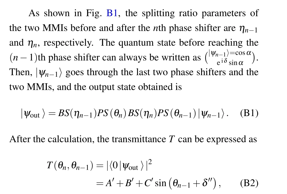
Appendix B:The case of different splitting ratios of MMIs
where
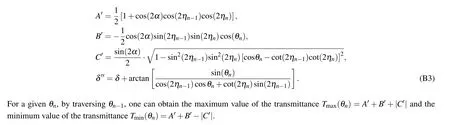

Fig.B1. The photonic circuit with cascaded phase shifters. Different MMIs have different splitting ratio parameters η0,η1,...,ηn-1 and ηn.
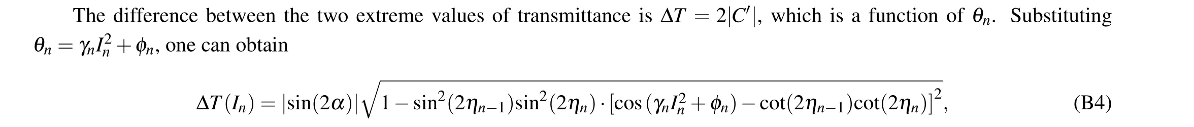
whereα,ηn,ηn-1,γn, andφnare all constants to be determined. The currentInis varied experimentally, and for eachIn, traverseIn-1to measure the maximum and minimum values of the transmittance and calculate their difference ΔT.The data of ΔTandInare then fitted using Eq.(B4),and the values ofα,ηn,ηn-1,γnandφncan be determined,thus completing the calibration of thenth phase shifter. The remaining phase shifters can be calibrated sequentially in the reverse order in a similar way.
Acknowledgements
Project supported by the National Key Research and Development Program of China(Grant No.2017YFA0305200),the Key Research and Development Program of Guangdong Province, China (Grant Nos. 2018B030329001 and 2018B030325001),and the National Natural Science Foundation of China(Grant No.61974168).
猜你喜欢
现代装饰(2021年5期)2021-12-02
读写月报(高中版)(2021年7期)2021-07-01
小学生学习指导(中年级)(2021年3期)2021-04-06
现代装饰(2019年11期)2019-12-20
初中生写作(2019年10期)2019-09-10
老友(2019年4期)2019-05-10
现代养生·上半月(2019年4期)2019-03-31
当代陕西(2018年22期)2018-12-21
爱你(2017年6期)2017-02-23
小天使·六年级语数英综合(2016年7期)2016-05-14

- Chinese Physics B的其它文章
- A design of resonant cavity with an improved coupling-adjusting mechanism for the W-band EPR spectrometer
- Photoreflectance system based on vacuum ultraviolet laser at 177.3 nm
- Topological photonic states in gyromagnetic photonic crystals:Physics,properties,and applications
- Structure of continuous matrix product operator for transverse field Ising model: An analytic and numerical study
- Riemann–Hilbert approach and N double-pole solutions for a nonlinear Schr¨odinger-type equation
- Diffusion dynamics in branched spherical structure