
Optical properties of He+-implanted and diamond blade-diced terbium gallium garnet crystal planar and ridge waveguides
2022-11-21 09:35JiaLiYou游佳丽YuSongWang王雨松TongWang王彤LiLiFu付丽丽QingYangYue岳庆炀XiangFuWang王祥夫RuiLinZheng郑锐林andChunXiaoLiu刘春晓
Chinese Physics B 2022年11期
Jia-Li You(游佳丽) Yu-Song Wang(王雨松) Tong Wang(王彤) Li-Li Fu(付丽丽) Qing-Yang Yue(岳庆炀)Xiang-Fu Wang(王祥夫) Rui-Lin Zheng(郑锐林) and Chun-Xiao Liu(刘春晓)
1College of Electronic and Optical Engineering,Nanjing University of Posts and Telecommunications,Nanjing 210023,China
2Shandong Provincial Engineering and Technical Center of Light Manipulations&Shandong Provincial Key Laboratory of Optics and Photonic Device,School of Physics and Electronics,Shandong Normal University,Jinan 250014,China
3Jiangsu Province Engineering Research Center for Fabrication and Application of Special Optical Fiber Materials and Devices,Nanjing 210023,China
Terbium gallium garnet(Tb3Ga5O12,TGG)crystal can be used to fabricate various magneto-optical devices due to its optimal Faraday effect. In this work,400-keV He+ ions with a fluence of 6.0×10¹⁶ ions/cm2 are irradiated into the TGG crystal for the planar waveguide formation. The precise diamond blade dicing with a rotation speed of 2×10⁴ rpm and a cutting velocity of 0.1 mm/s is performed on the He+-implanted TGG planar waveguide for the ridge structure. The darkmode spectrum of the He+-implanted TGG planar waveguide is measured by the prism-coupling method,thereby obtaining the relationship between the reflected light intensity and the effective refractive index. The refractive index profile of the planar waveguide is reconstructed by the reflectivity calculation method. The near-field light intensity distribution of the planar waveguide and the ridge waveguide are recorded by the end-face coupling method.The He+-implanted and diamond blade-diced TGG crystal planar and ridge waveguides are promising candidates for integrated magneto-optical devices.
Keywords: TGG crystal,optical waveguide,ion implantation,precise diamond blade dicing
1. Introduction
With the rapid development of communication technology, short-distance information propagation has higher requirements for the volume, cost and integration of communication device. Optical waveguides can be adopted to fabricate multifunctional and miniaturized devices.[1,2]They are physical elements that confine electromagnetic waves in the micronscale structures based on the total reflection principle.[3]According to the dimensions of confinement light, they can be divided into planar waveguides and ridge waveguides.[4]A planar waveguide is usually composed of three layers of dielectric media. The refractive index of the upper layer and lower layer are smaller than that of the core layer wrapped in the middle. Furthermore, a ridge waveguide can confine the energy of light field in both horizontal direction and vertical direction.[5]It is easy to build a stable and reliable optical circuit system. Therefore, the ridge waveguide is more widely used in integrated optics, compared with the planar waveguide.[6]In short, as the basic building blocks of integrated optics and optical communication,the waveguides can act as the channel through which signal light is propagated,and thus bridging between the different devices.[7]
In 1968,ion implantation proved for the first time that it can induce the refractive index of the transparent medium to change and can be used to prepare an optical waveguide.[8]Then,extensive and in-depth researches have been carried out in this field.[9–12]Compared with the other techniques for the waveguide construction, ion implantation has many advantages,such as high processing precision,wide applicable temperature range, and strong repeatability.[13]In the irradiation procedure, the ions with the energy of some keV/MeV are used to bombard the target crystal in the implantor or accelerator. A series of interactions between the irradiation ions and the particles of the target crystal will occur. The implantation ions gradually lose their energy and finally stay in the target crystal,causing the properties(such as the refractive index) of the sample surface to change.[14]Then, the waveguide structure on the order of microns is formed. Furthermore,the depth of ion implantation into the target material and the thickness of the damage layer can be controlled by adjusting the energy and dose of implanted ions.[15]However, ion implantation can be used only to fabricate one-dimensional(1D)waveguides. To fabricate two-dimensional (2D) waveguides,ion implantation needs to be combined with other surface processing techniques, such as precise diamond blade dicing[16]and femtosecond laser ablation.[17]Owing to the high Mohs hardness of the diamond blade,the diamond blade with a fast rotation can dice long grooves on the surface of the planar waveguide.[18]The part between two parallel adjacent grooves is the ridge waveguide.
As optical communication puts forward higher requirements for the performances of waveguides,the search for more suitable host materials has become an urgent task.[19]Terbium gallium garnet(Tb3Ga5O12,TGG)is a kind of magnetooptical crystal. It has some unique advantages, such as large Verdet constant (35 rad·T-1·m-1), high thermal conductivity (7.4 W·m-1·K-1), and high laser damage threshold (>1 GW/cm2).[20,21]The Tb3Ga5O12crystal plays a vital role in Faraday rotators and optical isolators. Therefore,investigations on the optical characteristics of the TGG waveguide is of great significance in developing passive devices in the field of optical communications. The ion implantation,such as carbon and silicon ion implantation, has been adopted to manufacture 1D and 2D TGG waveguides.[22,23]However, the exploration of the planar waveguide and the ridge waveguide by the He+-ion implantation combined with the diamond blade dicing in the TGG crystal has not been reported to the best of our knowledge. In the present work, the fabrication and optical properties of planar waveguide and ridge waveguide in the TGG crystal by the He+-ion irradiation and the diamond blade dicing are discussed in detail. It provides the possibility for the development of TGG waveguides as integrated Faraday magneto-optical devices.
2. Experiments and simulations
The TGG crystal with a dimension of 10.0 mm×5.0 mm× 1.0 mm was purchased from CASTECH Inc. Its largest surface and the smallest surface were both optically polished for the waveguide fabrication and property measurement. The He+-ion implantation was carried out on one TGG crystal surface with an area of 5.0 mm×10.0 mm for the fabrication of the planar waveguide as shown in Fig. 1(a). The energy and dose of the He+ions were 400 keV and 6.0×10¹⁶ions/cm2,respectively. The He+-ion implantation was performed at room temperature at Jinan Jingzheng Electronics Co., Ltd.(China). For the formation of the 2D waveguide, the surface of the planar waveguide was diced by a resin-bonded diamond blade with a thickness of 200 μm as shown in Fig. 1(b). A ridge structure was fabricated into the structure with a width of 30 μm. In order to avoid cracks in the dicing process, the rotation speed and cutting velocity of the blade were set to be 2×10⁴rpm and 0.1 mm/s,respectively.
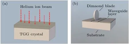
Fig. 1. Schematic diagrams of TGG waveguide fabrication, showing (a)He+-ion implantation and(b)precise diamond blade dicing.
The prism-coupling method (Metricon Model 2010,USA)was employed to measure the m-line curve of the planar TGG waveguide. A prism whose refractive index is 2.8648 at 632.8 nm was used to couple light into the optical waveguide from its polished surface with a width of 5.0 mm and a length of 10.0 mm. There was a thin air layer between the prism and the optical waveguide. When light was incident from the prism,evanescent waves were present in the air layer.If the incident angle of the beam was equal to a certain value,evanescent waves would enter into the waveguide. The dark-mode spectrum with some dips would be obtained at the same time.
The refractive index change of the host material induced by the implanted ions is affected by many factors, such as the parameters of the implanted ions and the property of the matrix substrate. Reflectivity calculation method (RCM) is a technique used to calculate the refractive index profile of the planar optical waveguide,based on the parameters of the darkmode characteristics(such as effective refractive index).In the simulation process,the parameters of the curve were continuously adjusted so that the difference between the simulated effective refractive index of the guided mode and the corresponding experimental datum is on the order of 10-3. Then,it is considered that the fitted refractive index distribution is close to the actual one.
The end-face coupling method was utilized to record the modal profiles of the planar waveguide and ridge TGG waveguide as shown in Fig. 2. An optical lens or microscope objective was used to focus the He–Ne laser(DH-HN250)light on the front end-face of the optical waveguide. After the light propagated in the waveguide, it was collected by the second lens or microscope objective. Finally, the guiding properties of the waveguide were characterized by the detection equipment such as a charge coupled device(CCD,CinCam CMOS-1201)and a power meter. In the experiments,the waveguides were placed on a three-dimensional (3D) motorized platform to achieve the precise adjustment of the waveguide positions.
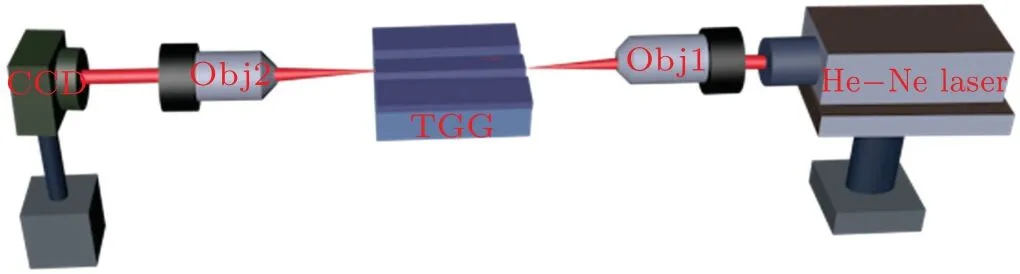
Fig. 2. Schematic diagram of end-face coupling system for recording the modal profiles of planar waveguide and ridge TGG waveguide.
3. Results and discussion
For exploring the mechanism of the planar waveguide formation and refractive index change, the SRIM 2013 software(Stopping and Range of Ions in Matter 2013)[24,25]is used to simulate the electronic energy loss and nuclear energy loss for the 400-keV He+-ion implantation into the TGG crystal as shown in Fig. 3. It can be seen that in an irradiation range of 0 μm–0.9 μm,the main energy loss is the electronic energy loss. Figure 3(a)shows that with approaching the sample surface,the electronic energy loss is greater. Its maximum value is 524.3 keV/μm. At a depth of 1.02 μm, the nuclear energy loss reaches a maximum value of 32.1 keV/μm as indicated in Fig.3(b),which is caused by the elastic collision between the irradiation ion and the nucleus of the target TGG crystal. In general,the ions disrupt the ordered structure of the lattice at the end of the irradiation range,resulting in a damage to layer in the crystal. An optical barrier will be formed at the end of the implantation range, resulting in the decrease of refractive index in this region.[26,27]
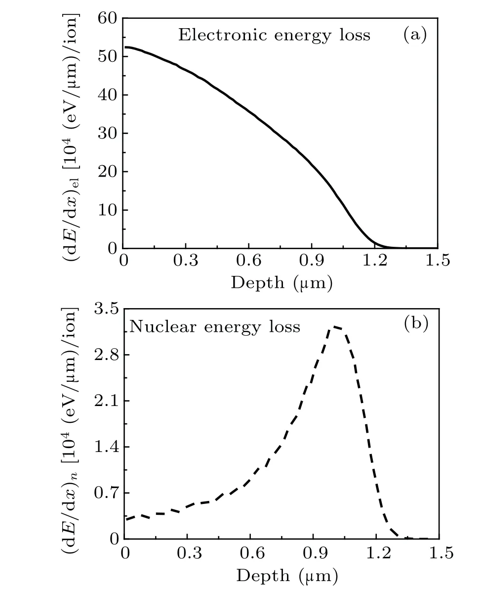
Fig.3.(a)Electronic energy loss and(b)nuclear energy loss for the 400-keV He+-ion implantation into the terbium gallium garnet crystal by the SRIM 2013 simulation.
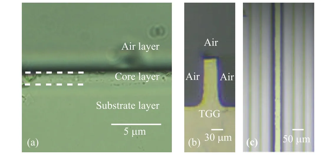
Fig. 4. (a) Micrograph of cross-section of planar waveguide, (b) end-face photograph,and(c)photo of surface of ridge TGG waveguide.
Figure 4(a) shows the microscopic image of the crosssection of the TGG planar waveguide taken by a metallographic microscope (Axio Imager A2m) under the transmission mode. The planar waveguide is about 1.08-μm thick,which is consistent with the range of the 400-keV He+-ion irradiation simulated by the SRIM 2013.Figures 4(b)and 4(c)show the photograph of end-face and surface of the ridge TGG waveguide measured by a Nikon microscope. As one can see,a pair of parallel air grooves with a lateral spacing of 30 μm is constructed on a 1D TGG waveguide after implementing the precise diamond blade dicing. Therefore,the light can be confined by the optical barrier layers(and the air layer)in the vertical direction and by the air grooves in the horizontal direction.
Dark-mode characteristics of the 400-keV He+-implanted TGG planar waveguide at TE mode is measured by the prism coupling system, and the results are shown in Fig. 5. Each dip in the dark-mode spectrum corresponds to a guided mode of the planar TGG waveguide. It can be seen that there are three dips at a wavelength of 632.8 nm. In practice,the effective refractive index is often used to characterize the angle of incidence. It is because the effective refractive index of the mode measured by the prism coupling system is a necessary parameter for fitting the refractive index profile of the waveguide by the RCM.[28,29]The first dip is sharp and represents the real guided mode, whose effective refractive index is 1.9464. The remaining two dips are relatively broad,indicating that they are the irradiation modes.[30–32]The refractive index of the TGG substrate is 1.9660, which is also measured by the prism-coupling method. By comparing the refractive index of the mode with th the substrate, it can be found that the effective refractive index of the guided mode is lower than that of the TGG substrate. It suggests that there may be an optical barrier with the reduced refractive index in the TGG crystal after implementing the ion implantation.[33]
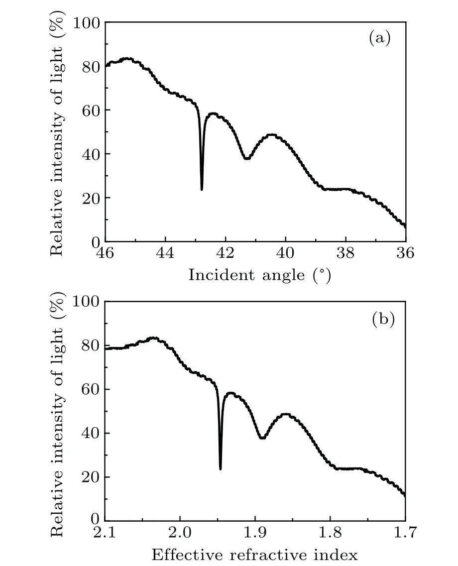
Fig.5. Relative intensity of light versus(a)incident angle and(b)effective refractive index for He+-implanted TGG waveguide.
The refractive index distribution of the 400-keV-He+-implanted TGG planar waveguide at 632.8 nm is reconstructed by the RCM[34,35]as shown in Fig. 6. From the figure,the maximum refractive index change is 0.02 at a depth of 1.06 μm. In addition, the surface refractive index is reduced by 0.006 from 0 to 0.7 μm. Therefore, the refractive index distribution of the He+-implanted TGG waveguide is of a typical “optical barrier” type. Therefore, the waveguide core is the layer from the TGG crystal surface to the optical barrier.Furthermore,the depth of the optical barrier calculated by the RCM is 1.048 μm, which is close to the value of 1.02 μm calculated by the SRIM 2013.
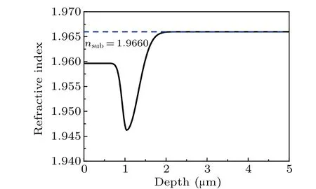
Fig.6. The refractive index profile of the He+-implanted TGG planar waveguide.
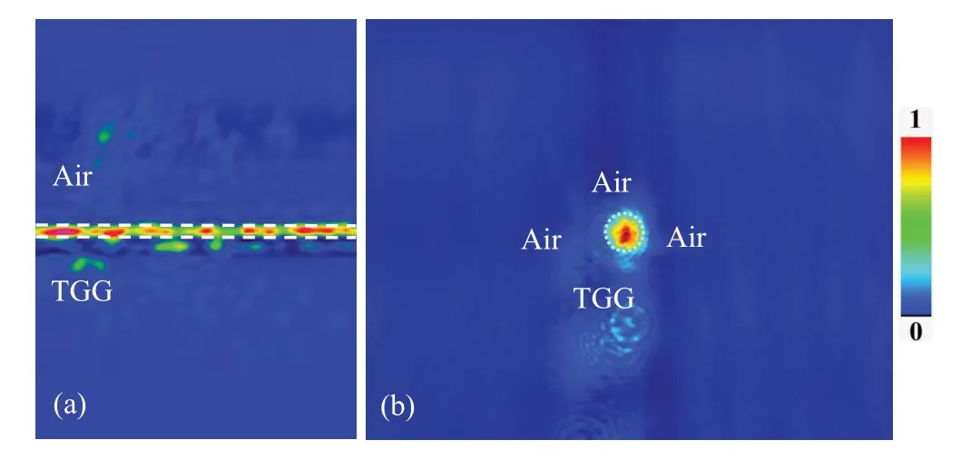
Fig.7. Near-feild light intensity distributions of(a)planar TGG waveguide and(b)ridge TGG waveguide.
The end-face coupling method is used to measure the near-field light intensity distribution at 632.8 nm for the planar waveguide and the ridge waveguide formed by the He+-ion implantation and the precise diamond blade dicing in the TGG crystal, as shown in Fig. 7. In Fig. 7(a), the planar waveguide fabricated by the He+-ion implantation can well support the propagation of light. That is to say,light can continuously and uniformly propagate in the planar waveguide. Furthermore, in Fig.7(b)the near-field light intensity distribution of the ridge TGG waveguide constructed by the combination of the He+-ion irradiation and the diamond blade dicing has a clear boundary and the light is completely distributed in the ridge structure. It indicates that the ridge waveguide confines the light propagation well and no light leaks into air and the substrate.In addition,the uneven distribution of the light propagation is caused mainly by the poor polishing of the end-face of the TGG crystal. Propagation loss is an important parameter to reflect the performances of a waveguide. Based on the end-face coupling system,the propagation losses of the planar TGG waveguide and the ridge TGG waveguide each with a length of 10 mm are estimated at 2.5 dB/cm and 2.9 dB/cm for the fundamental mode,respectively. The attenuation value of the ridge waveguide is larger than that of the planar waveguide,which is due to the roughness of the groove faces,induced by the diamond blade dicing process.[36,37]
4. Conclusions
The planar and the ridge waveguide structure are fabricated on the TGG crystal by a combination of the 400-keV He+-ion implantation with a fluence of 6.0×10¹⁶ions/cm2and the 0.1-mm/s diamond blade dicing with a rotation speed of 2.0×10⁴rpm. Based on the prism-coupling technique,there is one propagation mode on the m-line curve with an effective refractive index of 1.9464 for the planar waveguide.The refractive index of the planar waveguide core is 0.0014 higher than that of the optical barrier layer, according to the RCM simulation. The near-field light intensity distributions measured by the end-face coupling method suggest that the planar waveguide and the ridge waveguide can confine light propagation in the 1D direction and 2D direction with good guiding performances,respectively.They have the potential to server as Faraday rotators and waveguide isolators.
Acknowledgements
Project supported by the Postgraduate Research and Practice Innovation Program of Jiangsu Province, China(Grant No. SJCX21 0274), the National Natural Science Foundation of China (Grant Nos. 11405041 and 61905119),the Scientific Research Foundation for Youths Supported by Jiangxi Province Science Foundation, China (Grant No. 20192BAB217015), and the University Natural Science Research Project of Jiangsu Province, China (Grant No.19KJB140013).
猜你喜欢
中学生博览(2021年11期)2021-07-15
中学生博览(2021年13期)2021-07-14
中学生博览(2021年3期)2021-03-08
中学生博览(2021年1期)2021-03-04
艺术品鉴(2020年6期)2020-12-06
幼儿教育·父母孩子版(2020年8期)2020-03-04
环球人物(2018年19期)2018-10-17
中学课程辅导·教学研究(2017年11期)2017-09-23
西江文艺(2017年15期)2017-09-10
西江文艺(2017年15期)2017-09-10

- Chinese Physics B的其它文章
- A design of resonant cavity with an improved coupling-adjusting mechanism for the W-band EPR spectrometer
- Photoreflectance system based on vacuum ultraviolet laser at 177.3 nm
- Topological photonic states in gyromagnetic photonic crystals:Physics,properties,and applications
- Structure of continuous matrix product operator for transverse field Ising model: An analytic and numerical study
- Riemann–Hilbert approach and N double-pole solutions for a nonlinear Schr¨odinger-type equation
- Diffusion dynamics in branched spherical structure