Interface modulated electron mobility enhancement in core–shell nanowires
Yan He(贺言) Hua-Kai Xu(许华慨) and Gang Ouyang(欧阳钢)
1College of Science,Guangdong University of Petrochemical Technology,Maoming 525000,China
2Key Laboratory of Low-Dimensional Quantum Structures and Quantum Control of Ministry of Education,Key Laboratory for Matter Microstructure and Function of Hunan Province,School of Physics and Electronics,Hunan Normal University,Changsha 410081,China
The transport properties of core–shell nanowires(CSNWs)under interface modulation and confinement are investigated based on the atomic-bond-relaxation(ABR)correlation mechanism and Fermi’s golden rule.An analytical expression for the relationship between carrier mobility and interface mismatch strain is derived and the influence of size,shell thickness and alloyed layer on effective mass, band structures, and deformation potential constant are studied. It is found that interface modulation can not only reduce the lattice mismatch to optimize the band alignment, but also participate in the carrier transport for enhancing mobility. Moreover, the underlying mechanism regarding the interface shape dependence of transport properties in CSNWs is clarified. The great enhancement of electron mobility suggests that the interface modulation may become a potential pathway to improving the performance of nanoelectronic devices.
Keywords: core–shell nanowires,interface modulated,electron mobility
1. Introduction
Core–shell nanowires (CSNWs) have drawn significant attraction due to their outstanding electronic and transport properties, which provide a really possibility for improving the performance of catalytic, field effect transistors, and photovoltaic devices.[1–3]To date, an abundance of reports, experimental and theoretical,have shown that the epitaxial layer of shell can not only decay the surface state and defects to reduce the impurity and phonon scattering,[4,5]but also offer a radical channel for the rapid transport and separation to carriers for enhancing carrier collection efficiency.[6,7]However, some results are anxious for the unimaginably tunable interface phonon scattering and band structures induced by the lattice mismatch between core and shell parts,which exert an important influence on the performance of nanoelectronic devices.[8,9]Therefore, understanding the influence of interface strain on the transport properties and designing an optimized interface structures to achieve the sharpness interface in CSNWs become significant challenging problems in fundamental scientific and technological applications.
In general,the bottom-up approach is required for achieving a uniform coating of the shell materials during the particle formation and the core–shell transition can occur discontinuously (a “hard” interface) or may expect to be accompanied by interdiffusionions at the interface to smooth the confinement potential (called “interface engineering”), resulting in forming an alloyed transition region(a“soft”interface).[10,11]Nanowires (NWs) with hard or soft interfaces can have different transport and dynamical properties. Atomic-bondrelaxation (ABR) correlation mechanism[12,13]reveals that since a hard interface in CSNWs provides an additional driving induced by lattice mismatch and imperfect coordination numbers(CNs)that forces the interface atoms to deviate from intrinsic position, the mismatch strain and strain energy will take place.The magnitude of the strain energies determined by size,shell thickness and lattice parameters,and it may involve in chemical bonds to modify the Hamiltonian and band structure or even modulate the morphology to induce the charge redistribution.[14,15]Moreover,a sharpness interface modified by the interface modulation to form a soft interface will have less mismatch strain and strain energy as the lattice parameters changes gradually.[16]Contributions have shown that the alloying layer can reduce or eliminate the mixing of conductionband and valence-band to provide a more gradual change in the confinement potential for optimizing the band structure and eventually to improve the charge injection or collection at interface.[17–20]
Additionally, some studies shave revealed that the interface morphology modulation also plays a significant role in the carrier behaviors as it may provide a large interface area.[21,22]However,although considerable efforts have been made to investigate the effects of sharpness and softness interface on optical and electronic properties, the investigation of the influence of interface modulation on transport properties is still limited by two aspects. (i) Some one attempts to clarify that the epitaxial layer can participate in the carrier transport and provide a strong response to gate biasviathe Stark effect due to the lattice mismatch at the core–shell interface,[23]but there is a lack of quantitative calculation for the transport properties improving with the thickness of epitaxial layer increasing. (ii)Even though experimental measurements and theories have confirmed that the alloyed layer can reduce the interface lattice mismatch strain to optimize the band alignment and improve the carriers’lifetime,[24]the quantitative relationship between mismatch strain and transport properties is unclear. Therefore,in order to evaluate the influence of interface mismatch modulation on the transport properties of CSNWs and establish the relationship between theirs, we propose an analytical model to clarify the effects of size, shell thickness and alloy layer on effective mass,band structure and formation potential constant based on the ABR correlation mechanism and Fermi’s golden rule. The results show that the soft interface is helpful in blocking the phonon scattering and also in increasing the electron mobility as it decays the lattice mismatch strain,which may optimize the band structures and the participation in the carrier transport.Moreover,the difference between electron mobilities in CSNWs with cylinder and elliptic interface are also compared.
2. Principle
Physically,the transition rate for an electron in an initial statekto a final statek′can be calculated in terms of Fermi’s golden rule[25,26]

where ¯hωkand ¯hωk′ are the electron energy of initial state and final state,¯hωqis the phonon energy,Mk′kis the transition matrix elements,ψk= eik·ruk(r) is the wavefunction of a specific state,andV(r)is the scattering potential.
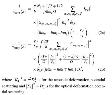
Generally, the above equation can be solved by the deformation potential theory and virtual-crystals approach.[27,28]By using the effectivemas approximation and the electron–phonon scattering mechanism,the relaxation time involves in an integral equation(see section S1 in the supporting information for details)and is expressed as

The acoustic deformation potential is proportional to the stretching-induced band-edge shift. We consider ΔEC, which is the conduction-band-edgeupward shift, while ΔEVis the valence-band-edgedownward shift. According to the thermodynamic approach,[29,30]we have (see section S2 in the supporting information for details)

wherem*eandm*hare the effective mass of electron and hole,respectively.
Moreover, for the AxB1-xalloy at the interface of A/B core–shell nanowires, the band edge energy can be approximated as[28]

whereEAandEBare the band edge energy of A and B,respectively,andxis the concentration of A atoms of AxB1-xalloy.Additionally,the electron effective massm*is the electron effective mass,specifically,

whereEis the electron energy. Moreover, the interaction of long-wavelength longitudinal–vibrational modes with the longitudinal-collective excitations becomes important when the free-carrier plasmon frequencyωpapproaches to the LOphonon frequencyωiwherem*=ne2/ω2pε0ε∞,[31]nandeare the electron concentration and electronic charge,ε0andε∞present are the permittivity of free space and high frequency dielectric constant, respectively. According to the ABR correlation mechanism,the dielectric constant relates to the band gapEgof specimen,andEg/EBg=f(D),[32]f(D)is a function of size andEBgdenotes the band gap of bulk case. Therefore,the effective mass with size and shell thickness can be deduced as follows:

whereεBandxmare the bulk dielectric constant and molar ratio,zi(zb) andEi(Eb) represent the coordination number and single bond energy ofi-th layer(bulk), ¯zandEc-sdenote the average coordination number and formation enthalpy of an interfacial bond,γiandγintare the surface-to-volume ratio(SVR)and interface-to-volume ratio,zrr(Err),zθθ(Eθθ),andzzz(Ezz)are the CNs(single bond energy)in the radial direction,the tangential direction,and the axial direction.
Therefore, the change of deformation potential constantDawith the influence of shell and alloy layer can be expressed as

whereεRis the lattice strain induced by the size effect (see section S2 in the supporting information for details), Δais a small change of lattice constant that results in a position shift ΔEin the energy band near the Fermi surface.
Consequentially, considering the discrepancies of transport properties between core and interface of AxB1-xalloy layers, the mobility of core can be given by a weight factors=Salloy/(Salloy+Score),whereSalloyandScoreare the area of alloy and the area of core. Thus,

3. Results and discussion
In order to clarify the influence of epitaxial layer and geometric shape on the transport properties,Si/Ge core–shell NW with an interface Si0.5Ge0.5alloy layer is considered. Moreover,to solve the Eq.(2),we consider that the relaxation time that involves in an integral equation can be solved numerically,for the scattering of sub-bands is not important for the considered cases and the approximation works well for the lowest sub-band which is the main contributor to mobility.[33]Therefore, we expect the main difference in comparison with the different wires to come from the deformation potentials.
Figure 1 shows the curves of size-dependent effective mass in various orientations of Si NWs. Evidently,m*increases with the decrease of diameter of Si and thickness of epitaxial layer. Those results are similar to other results that the electron effective mass of semiconductors is observed to decrease with band gap increasing.[34]Moreover, the results indicate that the existence of shell can not only reduce the quantum effect and Coulomb interaction,but also diminish the surface state and CNs defects,resulting in enhancing the cohesive energy and reducing the periodic potential and the effective mass. In our case,there are a lot of dangling bonds in the surface of bare nanostructures, which play an important role in its physical and chemical properties. However,an epitaxial layer coated on the surface of nanostructure is of great benefit to reducing the dangling bonds. As a result,the CNs’defects on the surface and surface state of the nanostructures will decrease dramatically. Our predictions are consistent with those in Refs.[35,36],whereas they deviate from some calculations due to the discrepancy between approximate methods.

Fig.1.Size-and shell-dependent effective mass of Si NWs,with inset showings schematic illustration of Si/Ge core–shell NWs.
The influence of interface modulation on band edge energy is studied, figure 2(a) shows the conduction-band-edge upward shift and valence-band-edge downward shift with size increasing, and the shift of bands decreases with shell thickness increasing.Our result is exceedingly well agreement with earlier result. Moreover,the shift of band edges suggests that the deformation potential constant may change with dimensionDand thickness of epitaxial layerHas shown in Fig.2(b).Clearly,the deformation potential constant decreases with core diameter and shell thickness increasing,and it approximates to 9.3 eV which is close to earlier result,9.5 eV.[37]The deformation potential constant is expected to increase since the effective mass approximation has been reported to be ΔE∝D-2,[38]while ABR correlation mechanism proposed that the lattice strain can be expressed asε=Δa/a∝D-1dependence.[39]As a result, the relationship between deformation potential constant and size should satisfyDa∝D-1.Moreover,the decrease ofDaunder a shell coated in Si NWs may be attributed to the reduction of strain. In fact,ΔE∝ΔEcoh∝ε2ζ,[30,39]whereεζis the strain of the core in the radial direction,the tangential direction,and the axial direction(see section S2 in the supporting information for details),then we haveDa∝εζ. Moreover,our results exhibit that the interface Si0.5Ge0.5alloy layer has an effect on the inhibiting of the deformation potential constant due to the reduction of mismatch strain at interfaceviastrain modulation in core–shell NWs with modulating lattice mismatch. The predictions imply that the epitaxial layer and interface alloy play a significant role in the transport properties of NWs.
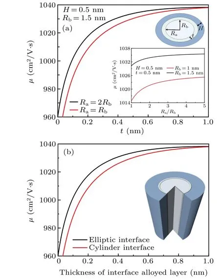
Figure 3 shows the curves of mobility of Si NWs as a function of NWs diameter, shell thickness, and alloy layers under various directions. As indicated in Fig. 3(a), mobility decreases with diameter declining. The results demonstrate that the scattering rate determined by electronic structure and mechanical structure,resulting in the different transport properties in the orientations of various crystals due to the discrepancy of effective mass,process of electron transition between energy levels,velocities,etc. Those trends are expected to be due to the wave form factor overlap increasing with diameter decreasing, which may enhance the phonon scattering in NWs. In particular,our results show that the influence of epitaxial layers exert a significant effect on the transport properties of NWs in small size. This trend is similar to the earlier results,but slightly larger.[27,37,40]In order to clarify the transport properties of NWs modulated by interface modulation,figure 3(b) shows the electron mobility as a function of alloy Si0.5Ge0.5thicknesst,with diameterDand thicknessHfixed.We find that the increase ofμcan be attributed to the decrease of mismatch strain and scattering rate. In our case, although epitaxial layer is of great benefit to the decreasing of the surface coordination bonds and surface states,the interface effect and lattice strain will occur as the discrepancy between the lattice constants in core Si and shell Ge.[41,42]The alloying layers may decay or even eliminate the interface effect and lattice mismatch between Si and Ge,resulting in optimization of the band structure of core. Additionally,since the SiGe alloy has a different electronic structure from Si,it can offer a real possibility for optimizing band structures and reducing scattering rate. Note that we may overestimate the carrier mobility due to the fact that the calculations did not take into account the intervalley scattering or alloy scattering.[43]
To further understand the influence of interface modulation on transport properties, CSNWs with elliptic interfaces are deliberately considered as shown in the inset of Fig.4.The transport properties of Si NWs with cylinder and elliptic interface are compared in Fig.4,and we find the NW with elliptic interface exhibits more excellent electron mobility. The reason may be due to the difference between mechanical structure and electronic structure induced by the SVR. In fact, on the one hand, Si NW with elliptic interface has lower SVR than that of cylinder interface, which suppresses the size effect and quantum effect to disturb the Hamiltonian. On the other hand,since the elliptical interface in core/shell NW has a wider range of interface extension than that of cylinder interface, more donors will provide Si core with alloy layer for taking part in the carrier transport.

Fig.4. Curves of change of electron mobility with thickness of alloy layer in Si/SiGe/Ge core–shell NWs with elliptic interface,with inset showing the schematic illustration of Si/SiGe/Ge core–shell NWs with elliptic interfaces and electron mobility of Si NWs versus Ra/Rb.
Additionally,as indicated in the inset of Fig.4,the electron mobility of Si NWs with elliptical interface demonstrates a first rapid increase with size increasing and then it become a constant whenRa/Rb>4. This result may be due to the fact that the electron mobility of elliptic interface withRa/Rb>4 can be treated as a two-dimensional phonon scattering rather than one-dimensional scattering as the transformation effect from one-dimensional to two-dimensional structures.
4. Conclusions
In this work, we proposed an analytical model to clarify the influence of interface modulation on the transport properties of core–shell NWs based on Fermi’s golden rule and ABR correlation mechanism. Our results indicate that the size and shell thickness exert a significant effect on phonon scattering and transport properties as the deformation potential constant and band structure change. We find the thick size and epitaxial layer reduce the surface state and wave overlap, resulting in the increase of electron mobility. In particular, the core/alloying/shell NWs,leading to the“smoothing”confinement potential, can dramatically enhance the transport properties of NWs as the alloy layer can decay or even eliminate the interface effect and lattice mismatch to optimize the band structures and participate in the carrier transport. Moreover,benefited from the low SVR and wider range of interface extension in elliptic interface, NWs with elliptic interface exhibits more excellent electron mobility than that of cylinder interface.
Acknowledgements
Project supported by the National Natural Science Foundation of China (Grant Nos. 91833302 and U2001215),the Guangdong Basic and Applied Basic Research Foundation, China (Grant No. 2022A1515010989), and the Special Project in Key Fields of Guandong Universities,China(Grant No.2022ZDZX3015).
- Chinese Physics B的其它文章
- A design of resonant cavity with an improved coupling-adjusting mechanism for the W-band EPR spectrometer
- Photoreflectance system based on vacuum ultraviolet laser at 177.3 nm
- Topological photonic states in gyromagnetic photonic crystals:Physics,properties,and applications
- Structure of continuous matrix product operator for transverse field Ising model: An analytic and numerical study
- Riemann–Hilbert approach and N double-pole solutions for a nonlinear Schr¨odinger-type equation
- Diffusion dynamics in branched spherical structure

