
TiO2/SnO2 electron transport double layers with ultrathin SnO2 for efficient planar perovskite solar cells
2022-11-21 09:40CanLi李灿HongyuXu徐宏宇ChongyangZhi郅冲阳ZhiWan万志andZhenLi李祯
Chinese Physics B 2022年11期
Can Li(李灿), Hongyu Xu(徐宏宇), Chongyang Zhi(郅冲阳), Zhi Wan(万志), and Zhen Li(李祯)
State Key Laboratory of Solidification Processing,Center for Nano Energy Materials,School of Materials Science and Engineering,Northwestern Polytechnical University,Xi’an 710072,China
The electron transport layer(ETL)plays an important role on the performance and stability of perovskite solar cells(PSCs). Developing double ETL is a promising strategy to take the advantages of different ETL materials and avoid their drawbacks. Here, an ultrathin SnO2 layer of ~5 nm deposited by atomic layer deposit (ALD) was used to construct a TiO2/SnO2 double ETL, improving the power conversion efficiency (PCE) from 18.02% to 21.13%. The ultrathin SnO2 layer enhances the electrical conductivity of the double layer ETLs and improves band alignment at the ETL/perovskite interface,promoting charge extraction and transfer. The ultrathin SnO2 layer also passivates the ETL/perovskite interface,suppressing nonradiative recombination. The double ETL achieves outstanding stability compared with PSCs with TiO2 only ETL.The PSCs with double ETL retains 85%of its initial PCE after 900 hours illumination. Our work demonstrates the prospects of using ultrathin metal oxide to construct double ETL for high-performance PSCs.
Keywords: atomic layer deposit,TiO2,SnO2,electron transport layer,stability
1. Introduction
Perovskite solar cells (PSCs) have attracted great attention since their discovery in 2009.[1]It is considered an ideal candidate for the next-generation low-cost photovoltaics. The perovskite materials possess excellent optoelectronic properties,such as high absorption coefficient,defect tolerance,and tunable bandgap, which enables the rapid development of PSCs.[2–7]Currently, the record power conversion efficiency(PCE) of PSCs has reached 25.8%,[8]comparable to that of silicon solar cells. Further development focuses on improving the performance and stability of the PSCs to realize their commercial applications.
The PCE of PSCs depends on many factors,including the quality of the perovskite film,[9–13]defects at the perovskite interface,[14–18]and the properties of the carrier transport layers.[19–29]Especially, the electron transport layer (ETL)plays a vital role on the performance of the PSCs. Firstly,the surface property of the ETL directly influences the nucleation and growth process of the perovskite films.Secondly,the electrical properties of the ETL strongly influence the electron extraction and transport process. Thirdly, the defects at the ETL/perovskite interface and the chemical reactivity of the ETLs have profound impacts on the stability of PSCs.
TiO2as a conventional electron transport material in the dye sensitized solar cells, has been employed in PSCs from the early research.[30]TiO2with different crystallinity, morphology and fabrication methods have been intensively investigated in the PSCs.[31–34]However, the PSCs with TiO2ETLs showed severe instability issue as a consequence of the high chemical reactivity of TiO2under UV light. To address this issue, alternative metal oxide based ETLs are developed. SnO2is an attractive ETL in planar PSCs attributed to its higher carrier mobility,lower conduction band maximum(CBM) and smaller photooxidation tendency.[35–37]Developing TiO2/SnO2double layer ETL combines the advantages of both TiO2and SnO2. Kong and coworkers deposited an amorphous SnO2layer on top of TiO2by solution process for PSCs,and achieved a best PCE of 21.4%.[38]Gaoet al.fabricated TiO2/SnO2double ETL by spin-coating SnO2nanoparticles on the TiO2layer,yielding a PCE of 18.85%.[39]Few reports have investigated the influence of the thickness of SnO2layer in the double layer on the performance of the PSCs in a comprehensive way. Atomic layer deposit(ALD)approach is a sequential,self-limiting,and layer-by-layer process,which produces film with thickness of several nanometers without pinholes. It is highly suitable for understanding the influences of the compact and ultrathin SnO2layer in the double layer ETLs on the performance and stability of the PSCs.
Here, we developed an ultrathin SnO2layer to construct a TiO2/SnO2double ETL for the planar PSCs. The ultrathin SnO2layers deposited by ALD process were 3–8 nm thick with outstanding compactness. With the TiO2/ultrathin-SnO2double ETL,the PCE of the PSCs was significantly improved from 18.02%to 21.13%. The PCE of double ETL based PSCs highly depends on the thickness of the ultrathin SnO2layer.Additionally, the ultrathin SnO2layer protects the perovskite from photocatalysis of TiO2layer. The PSCs with the double ETL retained 85% of its initial PCE after 900 hour continuous illumination. While the PCE of PSCs with TiO2only ETL quickly decayed to 64%. Our work demonstrates the prospect of employing ultrathin SnO2film to enhance the performance and stability of PSCs.
2. Methods
2.1. Materials
The 2,2′,7,7′-tetrakis-(N,N-di-4-methoxyphenylamino)-9,9′spirobifluorene) (Spiro-OMeTAD,99.9%), tris(2-(1Hpyrazol-1-yl)-4-tert-butylpyridine)-cobalt(III)tris(bis (trifluoromethylsulfonyl)imide)(FK209,99%),bis(trifluoromethanesulfonyl)imide(Li-TFSI,99%)and 4-tert-butyl pyridine(tBP,96%) were purchased from Xi’an Polymer Light Technology Corp. Tetrakis(dimethylamido)tin(TMDASn)was purchased from KE-MICRO,Jiaxing.Formamidine iodide(FAI,99.9%),methylammonium chlorine (MACl, 99.9%) and methylammonium bromine(MABr,99.9%)were purchased from Great cell. Lead iodide (PbI2, 99.9%) were purchased from TCI.Dimethylformamide (DMF,>99.9%), dimethyl sulfoxide(DMSO,99.9%),chlorobenzene(CB,99.9%)and acetonitrile were purchased from Sigma-Aldrich. All the reagents were used as received without any further purification.
2.2. Precursor solution preparation
The TiO2precursor solution(40 mmol/ml)was prepared by dissolving 900 μL TiCl4in 200 mL water.For the PbI2precursor solution, the PbI2powder was dissolved in the mixed solvent of DMF and DMSO(the volume ratio of 9:1)to form a solution of 1.5 M.For the FAI,MABr,and MACl precursor solution, FAI (90 mg), MABr (9 mg) and MACl (9 mg) was dissolved in 1 ml isopropanol. The hole transport layer(HTL)solution was prepared by dissolving 80 mg spiro-OMeTAD,34 μL tBP, 24 μL Li-TFSI (520 mg/mL in acetonitrile) and 9 μL FK209(320 mg/mL in acetonitrile)in 1 mL chlorobenzene.
2.3. Device fabrication
The FTO substrate was cleaned by surfactant, deionized water, acetone, isopropanol, and ethanol successively. After dried by the nitrogen gas, the FTO substrate was treated by UV-ozone for 15 min. To fabricate the TiO2layer by chemical bath deposit,the FTO substrate was immersed in the TiCl4aqueous solution(40 mmol/mL)and heated at 70°C for 60 min. The FTO substrate was then rinsed with deionized water and ethanol sequentially, and then annealed at 200°C for 30 min to obtain the TiO2compact layer.
The FTO/TiO2substrate was then transferred to the chamber of T-ALD 100A system to fabricate the ultrathin SnO2layer. The chamber was evacuated to a low pressure at 0.1 torr. TMDASn was used as the Sn source and heated at 55°C and H2O was employed as the O source. The deposit temperature was set to 160°C.The deposit cycle was varied to tune the thickness of the SnO2layer. After the ALD process,the substrate was transferred to a nitrogen-filled glove box for the fabrication of the perovskite film.
The perovskite film was fabricated in a two-step approach. The PbI2precursor was first spun on to the double ETL layer at 2000 rpm for 30 s and then annealed at 70°C for 1 min. The FAI,MAI,and MACl mixed solution was then spun on to the PbI2film at 2000 rpm for 30 s in the N2-filled glovebox and then annealed at 150°C for 15 min in the air to complete the perovskite conversion process. Afterwards, the HTL precursor solution was spun onto the perovskite film at 3000 rpm for 30 s in the glovebox. Finally, 80 nm Au electrodes were thermally evaporated in vacuum.
2.4. Measurement and characterization
The SEM images were recorded by FEI NAVA 450. The UV-vis absorption spectra were measured by UV-vis spectrophotometer (Lambda 35). PL spectra were measured using an Ocean Optics QE Pro spectrometer with an excitation wavelength of 532 nm. TRPL spectra were obtained using a Horiba PPD 900 spectrometer with an excitation wavelength of 405 nm. XPS measurements were performed using a Shimadzu Kratos photoelectron spectrometer. Simulated AM 1.5G sunlight was generated by a solar simulator (Newport,Sol3A).The light intensity(100 mW/cm2)was calibrated by an ISO 17025-certified KG3-filterred silicon reference cell.TheJ–Vcharacteristics of PSCs were recorded by a Keithley 2400 source-measurement The scan speed was 0.1 V/s(-0.1 V to 1.2 V).The incident photoelectron conversion efficiency (IPCE) was measured by a quantum efficiency measurement system(Enli Tech, QE-R3011). The cyclic voltammetry(CV)measurement was carried out in a three-electrode system with Fe(CN)-3/-46aqueous solution as the electrolyte and saturated calomel electrode as the reference electrode.The CV curves were recorded by CHI 760D electrochemical workstation. For the light stability measurement, the unencapsulated devices were stored in the nitrogen-filled glovebox and illuminated continuously under an LED light source. The illumination intensity of the LED was calibrated to introduce aJSCin the PSCs equaling to theJSCunder simulated sunlight(100 mW/cm2,AM 1.5G).
3. Results and discussion
Figure 1(a) shows the schematic diagram of the double ETL fabrication process. Briefly, a TiO2compact layer was first deposited on the fluorine-doped tin oxide(FTO)by chemical bath deposition(CBD).An ultrathin SnO2layer was then deposited on TiO2using ALD process. The thickness of the SnO2was precisely controlled by the reaction cycles of the ALD process. Details of the TiO2and SnO2deposition are described in Section 2. Figure S1(a)shows the scanning electron microscopy (SEM) of TiO2layer on the FTO substrate.Since the TiO2layer has a thickness of only 25 nm measured from the profilometer,the FTO/TiO2retains the pristine morphology of the FTO substrate. The roughness of the substrate after TiO2deposition is 32.1 nm by atomic force microscopy(AFM) as shown in Fig. 1(b). The thickness of SnO2of one reaction cycle is calibrated by the profilometer(Fig.S2). The SnO2growth rate was approximately 0.0743 nm per ALD cycle. Therefore,the thickness of a typical SnO2layer with 70-cycle growth is around 5 nm. The ALD deposited SnO2layer exhibited outstanding conformality that the surface morphology of the ETL showed no obvious difference after SnO2deposition (Figs. S1(a) and S1(b)). The ALD SnO2layer filled the pinholes of the underlying TiO2layer. As a result,the surface roughness was slightly reduced to 31.2 nm after the SnO2deposition(Figs.1(b)and 1(c)).
One day as he sat by her side feeling very happy, he received news that his father was lying at the point of death, and desired to see him before his end

Fig.1. (a)The schematic diagram of the TiO2/SnO2 double ETL fabrication process(tetrakis(dimethylamido)tin,TDMASn). The AFM images of(b)TiO2 and(c)TiO2/SnO2. The water contact angle of(d)TiO2 and(e)TiO2/SnO2 double ETL.
X-ray photoelectron spectroscopy (XPS) was performed to characterize the composition of the TiO2/SnO2double ETL.Figure S3(a)demonstrates the full XPS spectrum of the double ETL. The full spectrum shows both strong Sn peaks and relatively weak Ti peaks. This indicates that the SnO2coating on the TiO2layer is thin enough to allow x-ray excited photoelectrons to penetrate through, given the penetration limit is only several nanometers. The Sn 3d spectrum is shown in Fig. S3(b). The peaks at 486.4 eV and 494.8 eV correspond to the binding energies of Sn 3d5/2and 3d3/2, representing the Sn(IV) valence state. The O peak at 529.5 eV (inset of Fig. S3(b)) comes from the Sn–O bonds.[40]XPS confirms that an ultrathin layer of SnO2is deposited on the surface of TiO2.[41]To investigate the compactness of SnO2layer,cyclic voltammetry measurements were performed with bare FTO,FTO/TiO2and FTO/TiO2/SnO2as the working electrode, respectively. Fe(CN)3/46 aqueous solution was used as the electrolyte and saturated calomel electrode as the reference electrode. The results are compared in Fig. S4. For bare FTO,a strong redox peak is observed indicating fast and efficient redox reaction at the FTO/solution interface. When the FTO substrate is coated with TiO2,the redox peak is suppressed due to the TiO2blockage effect. However, the redox peak is still resolvable because of the pinholes and leakage channel in the TiO2.The redox reaction is further suppressed by the ultrathin SnO2coating,indicating that the ultrathin ALD SnO2layer is compact and fills the pinholes in the TiO2ETL.[42]Herein, a TiO2/SnO2double ETL with an ultrathin but compact SnO2layer was successfully constructed using ALD process.
The ETL plays a significant role on the perovskite film quality because its morphology and wettability influence the nucleation and growth process of the perovskite crystals.[43]The wettability of the TiO2ETL was changed by the ultrathin SnO2layer coating. As shown in Figs. 1(d) and 1(e),the TiO2layer had a contact angle of 13.6°. The contact angle was reduced to 6.8°after SnO2deposition. The superior wettability of the double ETL facilitates the perovskite crystal growth to produce larger perovskite crystals and high-quality perovskite films. Figures S5(a)and S5(b)show the SEM images of the perovskite films deposited on the TiO2-only ETL and TiO2/SnO2double ETL,respectively. The perovskite film on TiO2/SnO2double ETL showed a larger grain size. The average perovskite grain size increases from 550 nm on TiO2to 640 nm on the TiO2/SnO2double ETL (Fig. S5(c)). The larger grain size would reduce grain boundary defects and enhance the optoelectronic properties of the perovskite films.
PSCs with the structure of FTO/ETL/perovskite/spiro-OMeTAD/Au were fabricated to investigate the effects of the ultrathin SnO2on the performance of PSCs. The schematic of the PSC structure is depicted in Fig. 2(a). The different functional layers are also labelled in the cross-sectional SEM images of PSCs in Fig.2(b). As the thickness of the ultrathin SnO2layer is less than 10 nm, it cannot be differentiated in the cross-sectional SEM images. It can be seen that the perovskite crystals are compact and well aligned on the substrate and grow through the film without horizontal grain boundaries. The contact between the double ETL and perovskite layer is continuous without cracks or voids. The intimate contact promotes efficient electron extraction and transport in the PSCs.[44]
The photovoltaic performances of PSCs with the TiO2and TiO2/SnO2ETLs are compared in Figs. 2(c) and 2(d).Figure 2(c) shows theJ–Vcurves of the champion devices.The PSCs with TiO2/SnO2double ETL exhibited an opencircuit voltage (VOC) of 1.12 V, short-circuit current density(JSC)of 24.49 mA·cm-2,and fill factor(FF)of 78.34%,yielding a high PCE of 21.13%. In comparison,the PSC with TiO2ETL yielded a best PCE of 18.02%.The statistical distribution of photovoltaic parameters of PSCs with TiO2and TiO2/SnO2ETLs are shown in Fig. S6. It can be seen that theVOC,JSCand FF were all improved by the double ETL.The corresponding incident photon-to-electron conversion efficiency (IPCE)spectra are shown in Fig.2(d). The quantum efficiency of the PSC with double ETL is higher than that of the TiO2based PSCs in the whole perovskite absorption range,explaining the higherJSCin theJ–Vcurves.
As aforementioned, the thickness of the ultrathin SnO2layer can be precisely controlled by the deposit cycles,which is the advantages of ALD over other deposit techniques. The thickness of the ultrathin SnO2layer for the double ETL was optimized to achieve the best PSC performance. Figures 3(a)and S7 show the statistical distribution of photovoltaic parameters of the PSCs with different SnO2thicknesses. It is observed that the PSCs with 5 nm-thick SnO2exhibited the highest PCE. To elucidate the effects of the SnO2thickness on the final PCE of the PSCs, the optical and electrical properties of the ultrathin SnO2were studied. The transmittance spectra of the double ETL with different SnO2thickness are shown in Fig.3(b). It is obvious that the transmittance of the double ETL is decreased when the SnO2thickness increases.Figure 3(c) shows the IPCE spectra of PSCs with different SnO2thickness. The IPCE results are consistent with theJ–Vcurves, exhibiting the highestJSCfrom the 5-nm thick SnO2based PSCs. When the SnO2thickness increases from 2 nm to 5 nm,the quantum efficiency in the range of 350 nm to 650 nm is increased. The higher quantum efficiency of 5 nm thickness SnO2-based PSC in the short wavelength may be due to the reduced surface recombination at the perovskite/ETL interfaces.When the thickness is further increased to 8 nm,the quantum efficiency becomes lower in the full absorption range which could be due to the lower light transmittance of the 8 nm SnO2.
The series and shunt resistances (RsandRsh) of PSCs with different ALD SnO2thickness are extracted from theJ–Vcurves. As shown in Fig. 3(d), theRsfirst decreases then increases slightly when the thickness of the ALD SnO2is increased from 0 to 8 nm,and the 5 nm SnO2device shows the lowestRs. TheRshincreases with larger ALD SnO2thickness and plateaus at above 5 nm. The higherRshof the double ETL can suppress the undesired leakage current and improve the PCE. The thickness of the SnO2in the double ETL was fixed to 5 nm with the best PSC performance in the following investigation and discussion.

Fig. 2. Photovoltaic performance of the PSCs with double ETLs. (a) The schematic of the device structure and (b) the cross-sectional SEM images of the PSCs with TiO2/SnO2 double ETL.(c)The J–V curves of the champion devices with TiO2 and TiO2/SnO2 based PSCs and(d)the corresponding IPCE spectra.
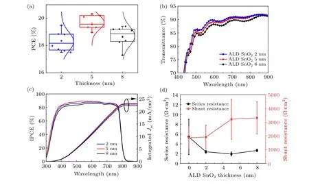
Fig.3. (a)The PCE distribution of the TiO2/SnO2 double ETL based PSCs with different SnO2 thicknesses;(b)the transmittance spectra of double ETL,(c)the IPCE spectra of PSCs,and(d)the series resistance and shunt resistance of the PSCs with the ultrathin SnO2 at varied thickness.
To understand the mechanism of PCE improvement by the double ETL, we further investigated the optoelectronic properties of the double ETL.Figure S8(a)shows the transmittance spectra of the TiO2and TiO2/SnO2ETLs. The transmittance was only slightly reduced between 400 nm and 450 nm due to the UV absorption of the SnO2layer. There was negligible absorption between 550 nm and 900 nm by the ultrathin SnO2. On the other hand, the SnO2layer showed strong impact on the electrical conductivity as shown in Fig.S8(b). The structure of FTO/ETL/Ag was fabricated to measure the film conductivity. The electrical conductivity was improved from 2.49×10⁻⁴S/cm of the single TiO2layer to 3.08×10⁻⁴S/cm of the double ETL.The better conductivity of the double ETL may be due to the smooth surface that improves the interface contact and better energy level of the ETL to form an ohmic contact.

Fig.4. Electrical and optoelectronic properties of the double ETLs: (a)the band structure of PSCs with the TiO2/SnO2 double ETL,(b)the Mott–Schottky analysis, (c)dark current density–voltage curves, and(d)space charge limited current(SCLC)characterization of perovskite films with TiO2 and with TiO2/SnO2;(e)steady-state PL spectra and(f)time-resolved PL spectra of perovskite films on TiO2 and TiO2/SnO2.
The band diagram of the PSCs with double ETL is depicted in Fig.4(a). The smaller conduction band energy offset between the double ETL and perovskite favors electron extraction from the perovskite films to the double ETL. The better band alignment between the double ETL and perovskite can improve the FF andJSCof the PSCs in consistent to theJ–Vresults. The built-in potential in the PSC was measured by Mott–Schottky to show the band alignment improvement by the double ETLs(Fig.4(b)). The built-in potential(Vbi)is determined from the intercept of the linear portion of the Mott–Schottky[45]plot with the potential axis from the following equation:

whereCis the capacitance,Nis the carrier density,∈0is the permittivity of free space,∈is the permittivity of the perovskite material,Ais the area of the PSCs,eis the elementary charge,andVis the applied voltage. The built-in potential increased from 0.87 V with TiO2-only ETL to 0.92 V with the double TiO2/SnO2ETL. The higher built-in potential is due to the larger energy offset between the HTL and ETLs, which is beneficial for carrier separation in the PSCs. The increase of the built-in potential contributes to theVOCimprovement in the PSCs. The darkJ–Vcurve of the PSCs was measured as shown in Fig. 4(c). It can be seen that the reverse saturation current was suppressed with the double ETL, owing to the reduced pin-holes in the ETL and better crystallinity of the perovskite film.
The space charge limited current (SCLC) measurements were conducted to characterize the defect density in the perovskite films.[46]The electron-only device was fabricated in the structure of FTO/double ETL (or TiO2)/perovskite/PCBM/Au and the current–voltage curve is shown in Fig.4(d). The defect density(Ntrap)of the electrons in the perovskite film can be calculated using the equation

wheredis the thickness of the perovskite film, andVTFLis the trap-filled limited voltage. TheVTFLof SCLC measurement for perovskite with TiO2and TiO2/SnO2were 0.51 V and 0.56 V, respectively. Therefore, the defect density of the perovskite film decreased from 2.23×1015cm-3with TiO2to 2.03×1015cm-3with TiO2/SnO2. Consequently,the double ETL enhanced the perovskite film quality and reduced the defects density at the ETL/perovskite interface contributing to the suppressed nonradiative recombination andVOCimprovement. The charge carrier dynamics was characterized by photoluminescence(PL).Figure 4(e)shows the steady-state PL of the perovskite films on TiO2and TiO2/SnO2. The perovskite PL intensity was reduced by the TiO2/SnO2due to more efficient electron extraction. The carrier lifetime decreased from 108.1 ns with TiO2to 81.5 ns with TiO2/SnO2fitted from the time-resolved PL spectra (Fig. 4(f)). The PL results suggest that the double ETL improves the electron extraction,matching with the better band alignment of the double ETLs. Overall, the TiO2/SnO2double ETL reduces the interface defects,improves the band alignment of the ETL/perovskite interface and contributes to the higher PCE in the PSCs.

Fig. 5. (a) The stabilized power output measurements of PSCs with TiO2 and TiO2/SnO2 double ETL; (b) the normalized PCE of PSCs with TiO2 and TiO2/SnO2 under continuous illumination.
The ultrathin SnO2based double ETL not only improves the PCE but also enhances the stability of the PSCs. Figure 5(a) shows the stabilized power output measurements of the PSCs with TiO2and TiO2/SnO2. The power output of the PSCs with double ETL exhibited negligible decay during the 1800 s measurement. However, the PCE of PSCs with only TiO2decreased quickly. The results suggest that the light stability of the PSCs is improved. Moreover, the light stability of the PSCs is further studied under continuous illumination.The PSCs with double ETL retained 85% of its initial PCE after 900 h continuous illumination without UV filter. On the contrary, the PCE of PSCs with TiO2-only ETL quickly decayed to 64% of its initial value. The different light stability may arise from the photocatalysis properties of the TiO2ETL. The high chemical reactivity of TiO2under UV-light leads to the degradation of perovskite materials. Although the ultrathin SnO2layer only has a thickness around 5 nm, the compact and pinhole-free features effectively protect the perovskite film from photocatalysis degradation caused by TiO2.
4. Conclusion and perspectives
In this work, we demonstrated an ultrathin SnO2layer based TiO2/SnO2double ETL for efficient and stable PSCs.The ultrathin SnO2layer fabricated by ALD process with a thickness of several nanometer modified the physical and chemical properties of the ETL significantly. The good wettability of the double ETL enhanced the perovskite grain size and film quality through promoting crystals growth. With an optimized SnO2thickness of 5 nm,the double ETL improved PCE of PSCs from 18.02%to 21.13%. The double ETL with enhanced electrical conductivity and reduced pin-holes led to lower series resistance and higher shunt resistance in the PSCs.The double ETLs also showed improved band alignments between ETL and perovskite which promotes the PSCs performance. The defects density at the ETL/perovskite interface was passivated by the ultrathin SnO2layer,leading to a higherVOCin the PSCs. Owing to the low chemical reactivity of SnO2under UV light,the PSCs with double ETL showed remarkable light stability, retaining 85%of its initial PCE after 900 h under continuous illumination. Our work demonstrates the potential of using the scalable ALD process to efficiently modify the ETL materials with ultrathin layers to achieve efficient and stable PSCs.
Acknowledgements
We would like to thank the Analytical & Testing Center of Northwestern Polytechnical University for SEM,XPS,UPS characterizations.
This work is supported by the National Key R&D Program of China (Grant No. 2019YFB1503201), the National Natural Science Foundation of China (Grant Nos. 52172238,52102304, 51902264, and 51902177), the Natural Science Foundation of Shanxi Province, China (Grant No. 2020JM-093),Joint Research Funds of Department of Science&Technology of Shaanxi Province and Northwestern Polytechnical University (Grant No. 2020GXLH-Z-014), Science Technology and Innovation Commission of Shenzhen Municipality(Grant No. JCYJ20190807111605472), and the Fundamental Research Funds for the Central Universities,China(Grant Nos.3102019JC0005 and G2021KY05103).

- Chinese Physics B的其它文章
- A design of resonant cavity with an improved coupling-adjusting mechanism for the W-band EPR spectrometer
- Photoreflectance system based on vacuum ultraviolet laser at 177.3 nm
- Topological photonic states in gyromagnetic photonic crystals:Physics,properties,and applications
- Structure of continuous matrix product operator for transverse field Ising model: An analytic and numerical study
- Riemann–Hilbert approach and N double-pole solutions for a nonlinear Schr¨odinger-type equation
- Diffusion dynamics in branched spherical structure