
Electron delocalization enhances the thermoelectric performance of misfit layer compound(Sn1-xBixS)1.2(TiS2)2
2022-11-21 09:40XinZhao赵昕XuanweiZhao赵轩为LiweiLin林黎蔚DingRen任丁BoLiu刘波andRanAng昂然
Chinese Physics B 2022年11期
关键词:刘波
Xin Zhao(赵昕) Xuanwei Zhao(赵轩为) Liwei Lin(林黎蔚) Ding Ren(任丁)Bo Liu(刘波) and Ran Ang(昂然)
1Key Laboratory of Radiation Physics and Technology,Ministry of Education,Institute of Nuclear Science and Technology,Sichuan University,Chengdu 610064,China
2Institute of New Energy and Low-Carbon Technology,Sichuan University,Chengdu 610065,China
The misfit layer compound(SnS)1.2(TiS2)2 is a promising low-cost thermoelectric material because of its low thermal conductivity derived from the superlattice-like structure. However,the strong covalent bonds within each constituent layer highly localize the electrons thereby it is highly challenging to optimize the power factor by doping or alloying. Here,we show that Bi doping at the Sn site markedly breaks the covalent bonds networks and highly delocalizes the electrons. This results in a high charge carrier concentration and enhanced power factor throughout the whole temperature range.It is highly remarkable that Bi doping also significantly reduces the thermal conductivity by suppressing the heat conduction carried by phonons,indicating that it independently modulates phonon and charge transport properties. These effects collectively give rise to a maximum ZT of 0.3 at 720 K.In addition, we apply the single Kane band model and the Debye–Callaway model to clarify the electron and phonon transport mechanisms in the misfit layer compound(SnS)1.2(TiS2)2.
Keywords: misfit layer sulfide,electron delocalization,carrier mobility,chemical bond
1. Introduction
Over 60%fossil fuels input for power generation is being rejected as low-grade heat annually.[1]Thermoelectric materials are able to directly convert such a huge amount of heat into utilizable electricity[2]without releasing any chemical residuals, showing great potential to contribute to solving the energy problem at present.[3,4]The efficiency of a thermoelectric device primary depends on the figure of merit, namely,ZT, of the thermoelectric materials used, which is defined asZT=S2σT/κtot,[4]whereSrepresents Seebeck coefficient,σdenotes electrical conductivity, their productS2σis called power factor,Tis the absolute temperature,andκtotis the total thermal conductivity with contribution from both charge carriers(κele)and phonons(κlat).
In the past decades, theZTvalues of representative thermoelectric compounds have been considerably improved by applying innovative strategies, such as optimizing electrical transport properties[5–10]or suppressingκlat.[11,12]However, the majority thermoelectric materials contain toxic or expensive elements. For extensive application, thermoelectric community currently puts interest on searching economically-viable, environmentally benign thermoelectric materials.[13–15]The surprising and promising examples are the discovery of Mg3Sb2[8,16–18]and SnSe[19–22]based compounds with intrinsically low thermal conductivity. The former shows exceptionally highZTvalue of~1.5 around room temperature,exceeded conventional expensive Bi2Te3.[8,16,17]The latter exhibits extraordinary performance over a broad temperature window. Besides, the study of the physical mechanisms of novel materials is also very important. The single crystal 1T-TaS2sample exhibits strong coupling between phonon excitation and commensurate charge-densitywave lattice,which provides a deep insight into close association between electronic correlation and dynamical motions of phonons.[23]These findings unambiguously highlight the importance of discovering new compounds.
(SnS)1.2(TiS2)2is an n-type misfit layer semiconductor built by alternately stacking two atomically thin TiS2slabs with a van der Waals (vdW) gap and SnS monolayer along theccrystallographic direction. Given the abundant interface formed between the TiS2and SnS layer,it shows intrinsically low thermal conductivity compared with other thermoelectric sulfides.[24,25]However, it is highly challenging to optimize its power factor because the metal cation easily forms covalent bonds with sulfur, highly localizing the electrons. For example, (Sn0.96Sb0.04S)1.2(TiS2)2shows carrier concentration nearly the same to the pristine one.[26]Here, we reveal that Bi doping can effectively improve the carrier concentration without degrading the carrier mobility by delocalizing the surrounding electrons. This gives rise to an enhanced power factor over the entire temperature investigated. Remarkably,the heavy Bi atom also significantly decreases the lattice thermal conductivity by generating point defects.[27]As a result,(Sn0.96Bi0.04S)1.2(TiS2)2shows aZTvalue of 0.3 at 723 K,one of the highest values reported in this compound.
2. Experimental details
2.1. Synthesis and sample preparation
The appropriate molar ratio of high purity elements of tin (99.99%, aladdin), titanium (99.99%, aladdin), sulfur (99.99%, aladdin) and bismuth (99.999%, aladdin) corresponding to (Sn1-xBixS)1.2(TiS2)2(x= 0,0.02,0.04,0.06)was sealed in a quartz tube under a high vacuum(~10-4Pa).To minimize the risk of explosion, the sealed tubes were slowly heated to 773 K and dwelled for 12 h, afterward the temperature was raised to 1073 K and allowed to react for 48 h,and naturally cooled down to ambient temperature. The obtained ingots were hand-ground into fine powders in air using an agate and pestle. The resulting fine powder was loaded into a graphite die mold and hot pressed at 923 K for 45 min under an axial pressure of 50 MPa in a dynamic vacuum. The density of the sample was determined by the geometrical dimensions and masses, showing all the samples have density higher than 97.3%of the theoretical value.
2.2. Powder x-ray diffraction
The pulverized samples were used for powder x-ray diffraction (XRD). The powder diffraction patterns were recorded with CuKα(λ=1.5418 ˚A) radiation in a reflection geometry on an Inel diffractometer operating at 40 kV and 20 mA (DX-2700 x-ray diffractometer). All measured samples are single phase within the detection limit of our laboratory XRD instrument,showing none of detectable secondary phases and unreacted elements.
2.3. Charge carrier transport
The densified samples were cut into different shapes using a wire saw for charge and thermal transport properties measurement respectively. The rectangular bar with the dimension of 2×3×8 mm3was used for simultaneously measuring the electrical conductivity and Seebeck coefficient employing a CTApro instrument under a low-pressure helium atmosphere from 320 K to 720 K.The Hall charge carrier concentration and mobility were measured from 320 K to 720 K by a home-built apparatus with a unidirectional 1.5 T magnetic field under a high vacuum.
2.4. Thermal conductivity
Thermal diffusivities with respect to temperature were measured using disks with a diameter of 6 mm or 8 mm and a thickness of 1.5 mm using the laser flash diffusivity method on a Netzsch LFA 467 instrument. The surface of the disks was protected by a thin layer of graphite to minimize the thermal radiation at elevate temperature. The thermal conductivity was calculated by the equationκtot=ρ·D·Cp,whereρis the mass density,Dis the measured thermal diffusivity, andCprepresents the temperature-dependent heat capacity that can be determined byCp= [0.17078+(2.64876×10⁻⁵)×T]J·g-1·K-1,whereTis the absolute temperature. The electrical contribution to the total thermal conductivity was calculated based on the relationκele=LσT,whereLis the Lorenz number estimated using a single parabolic band(see supporting information for the details),σis the electrical conductivity,andTis the absolute temperature. Lattice thermal conductivityκlatwas calculated by the relationκlat=κtot-κele.
2.5. Electronic structure calculation
The first-principles calculations were performed by utilizing the Perdew–Burke–Ernzerhof (PBE)[28]formalism and generalized gradient approximation (GGA)[29,30]implemented in Viennaab initiosimulation package (VASP)[31,32]code. The plane-wave basis was truncated at the energy cutoff of 600 eV. To reduce the computational load, we only sampled the momentum space at theΓ-point and a 4×1×1 mesh.All geometry structures were fully relaxed until the calculated Hellmann–Feynman force on every atom were less than 0.03 eV·˚A-1under the convergence condition of 10-4eV.
3. Results and discussion
Covalent bonds in(SnS)1.2(TiS2)2strongly trap the electrons so that softening these bonds may release the localized electrons. Note that, the bond dissociation energy for Bi–S is 315 kJ·mol-1, much lower than 467 kJ·mol-1for Sn–S and 387 kJ·mol-1for Sb–S.[33]This indicates Bi doping can weaken the covalent bonds and give rise to a higher carrier concentration than the Sb doped system. To verify our hypothesis,we synthesized samples with the composition of (Sn1-xBixS)1.2(TiS2)2(x=0,0.02,0.04,0.06) using hightemperature solid-state reaction.All the phases can be fully indexed as the misfit layer structure,showing neither detectable impurity phases nor unreacted residual within the resolution limit of lab XRD measurements (Fig. 1(a) and Fig. S1). To accurately determine the lattice parameter, we performed Rietveld refinement on the recorded XRD patterns(Fig.S2 and Table S1). The refined unit cell dimensions gradually shrink as the Bi content increases, suggesting that Bi atoms are homogenously dissolved over the matrix apparently (Fig. 1(b)).This finding agrees well with the microscopic elemental map collected by scanning electron microscopy equipped with an energy dispersive spectroscopy(SEM-EDS,Fig.S3).

Fig. 1. (a) Powder XRD patterns of (Sn1-xBixS)1.2(TiS2) samples (x =0,0.02,0.04,0.06). (b)Lattice parameters with respect to the Bi content.
Trivalent Bi3+substituting divalent Sn2+could increase charge carrier properties significantly. In accordance,we measured the temperature-dependent Hall carrier concentration and mobility for the (Sn1-xBixS)1.2(TiS2)2(x=0,0.02,0.04,0.06) samples. Note that although we measured all properties along both parallel and perpendicular to the hot press direction, we will mainly concentrate on those perpendicular to the press direction because it shows higherZT. The transport properties collected parallel to the press direction are shown in Fig.S4.As the concentration of Bi doping increases,we can see an enhancement of the electrical properties. This is consistent with the results observed in the in-plane, which also can confirm our hypothesis.
All samples show nearly constant Hall carrier concentration (nH) over the entire temperature range investigated, and their values monotonously increase with higher Bi concentration (Fig. 2(a)). It should be noted that the electron doping efficiency,namely,the number of electrons per Bi atom to the matrix is markedly higher than previously reported values for other dopants in(SnS)1.2(TiS2)-based materials. For example,x=0.04 sample showsnHof 1.8×1021cm-3at 300 K, indicating its electron doping efficiency amounts to 0.63 e-. In sharp contrast,(Sn0.96Sb0.04S)1.2(TiS2)exhibits annHclose to the matrix at 300 K as indicated by the green dashed line,[26]revealing Sb has negligible electron doping efficiency. These verify that Bi atom acts as an efficient electron donor to the(SnS)1.2(TiS2)lattice.

Fig.2. Charge transport properties of the(Sn1-xBixS)1.2(TiS2)2 samples(x=0,0.02,0.04,0.06). (a)Temperature-dependent Hall carrier concentration nH. The experimental data of(Sn0.96Sb0.04S)1.2(TiS2)2 from previously report is included for comparison(green dashed line).[26] (b)Temperature dependent Hall mobility μH, (c) conductivity σ and (d) Seebeck coefficient. (e) Carrier concentration-dependent Seebeck coefficient at 320 K and 720 K.(f)Temperature-dependent power factor.
Although Bi doping considerably increases thenH, it marginally reduces the charge carrier mobility (μH). In fact,all samples exhibit nearly identicalμHover the entire temperature range (Fig. 2(b)). Their values rapidly drop with the raising temperature, following the same power law trend of~T-1.5over the entire temperature range, which evident the phonon scattering dominates the charge carrier scattering.This observation confirms Bi uniformly spreading over the crystalline matrix,rather than forming secondary phases or aggregate at the grain boundary,otherwise theμHwould be significantly decreased. Indeed,it contrasts with the general understanding that increasing charge carrier concentration usually decreases with raisingnHbecause of enhanced carrier–carrier scattering, implying Bi doping marginally affects the charge carrier transport.
Figure 2(c) shows the electrical conductivity (σ) with respect to temperature for the (Sn1-xBixS)1.2(TiS2)2(x=0,0.02,0.04,0.06)samples. Because Bi doping markedly improves thenHwith negligible degradingμHin the full temperature range,it gives rise to higherσat every single temperature point compared to the pristine sample. For example,theσof the title compound(Sn0.96Bi0.04S)1.2(TiS2)is~1100 S·cm-1and~300 S·cm-1at 300 K and 723 K, respectively, much higher than~900 S·cm-1and 250 S·cm-1at the same temperature for the pristine sample.
The Seebeck coefficient(S)of all samples is negative over the entire temperature range, demonstrating they are n-type semiconductor(Fig.2(d)).Note that Bi doping marginally impacts the magnitude of Seebeck among samples because all the samples have very highnHon the order of~1021cm-3. To examine any possible modulation in electron effective massm*, we calculated the theoretical Pisarenko relation betweenSandnHfor undoped (SnS)1.2(TiS2) in the frame of single Kane band model by assuming that the phonon scattering governs the charge carrier scattering. The black and red lines denotem*=4meat 320 K andm*=5meat 720 K,respectively(Fig.2(e)).TheSvalues for all the samples in this work match well on the lines, suggesting that doped Bi does not alter the band structure in the vicinity of the Fermi level.
Due to the doped Bi considerably increasesσwithout significantly reducingS,it optimizes the power factor particularly for the best composition(Sn0.96Bi0.04S)1.2(TiS2)(Fig.2(f)).In fact,the(Sn0.96Bi0.04S)1.2(TiS2)sample shows a power factor higher than the pristine one over the entire temperature range.Note that it is challenging to improve the power factor of misfit layer compounds because the highly distorted interface derived from the constituent layers typically leads to a very low electrical conductivity and thereby a low power factor.
To better understand the enhanced charge transport properties in the (Sn1-xBixS)1.2(TiS2)2compounds, we carried out first-principles calculation within density functional theory regime. Given the high electron doping efficiency as we discussed earlier,the doped Bi atom was placed at the Sn site to mimic the experimental observation. We first analyzed the charge transfer in Bi doped (SnS)1.2(TiS2) for examining the possible charge transfer between Bi and the matrix. For clarity,we only display the charge transfer between one TiS2layer and its neighboring SnS slab(Fig.3(a)). The result shows that the electrons of Bi flow toward the nearest sulfur atom in the adjunct TiS2layer as indicated by the blue ellipsoid, forming electronic bridge to connect large van der Waals gap and facilitate the charge transfer over the matrix. For comparison,we also similarly calculated the Sb doped (SnS)1.2(TiS2). It reveals that the electrons from Sb atom are isolated between the van der Waals gap.
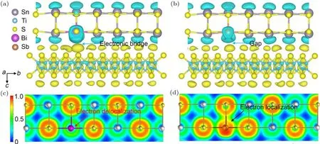
Fig.3. The charge transfer analysis for(a)Bi and(b)Sb doped(SnS)1.2(TiS2). The Sn,Ti,S,Bi and Sb atoms are depicted by grey,blue,yellow,violet, and orange spheres, respectively. Blue ellipsoids surrounding the atoms denote a loss of electrons. Electron localization function (ELF)contour mapped along the〈100〉zone axis for(a)Bi and(b)Sb doped(SnS)1.2(TiS2). ELF values ranging from 0 to 1 are depicted by the color bar shown in(c), where blue color denotes the electrons with almost no localization or no electrons, and the red color corresponds to the perfect localization of electrons. The red arrow in (c) indicates Bi substituting Sn delocalized electrons. The black arrow in (d) points out the Sb atom forms covalent bond with adjunct sulfur atom,which heavily localized the electrons.
It is worth noting that quantitative Bader charge transfer analysis shows that Bi donates 1.27 e-to the interacting S atom,coincidentally to the value of 1.28 e-of Sb transferred to the system. This supports our hypothesis that Bi doping weakly localized the electrons. We calculated the electron localization function(ELF)for both Bi and Sb doped systems(Figs.3(c)and 3(d)). This measures the electron localization in atomic and molecular systems, directly evaluating the chemical interaction between the adjunct atoms.[34]The magnitude of ELF increases from 0 to 1 which denotes the electron transiting from no localization to perfect localization and is visualized by the color code varying from blue to red color. The ELF contour mapped along the〈100〉zone axis of Bi doped system reveals the ELF value between Bi and S atoms smaller than 0.5 (Fig. 3(c)). This indicates that electrons surrounding Bi are highly mobile,consistent with our observation that incorporating Bi atom negligibly affectsμH.By contrast,electron localization domains are clearly observed between Sb and S atoms in Sb doped(SnS)1.2(TiS2)as indicated by the black arrow. This suggests that the Sb atom is prone to form covalent bond with nearby sulfur atom,trapping the free electrons and reducing the electron doping efficiency. In fact, the EFL results agree well with the fact that the Bi–S bond has lower enthalpy and dissociation energy than the Sb–S bond as we discussed in the previously section, confirming that the weak bond contributes to the exceptionally charge transfer of Bi.
Figure 4(a)presents temperature-dependent total thermal conductivity(κtot)for the(Sn1-xBixS)1.2(TiS2)2samples(x=0,0.02,0.04,0.06). It is highly remarkable that all Bi-doped samples show suppressedκtotcompared with the pristine sample despite they exhibit much higherσthan the latter.This observation implies that the Bi doping significantly impedes heat conduction by phonons. As a result, we extracted the lattice thermal conductivityκlatby invoking the Widemann–Franz law to subtract electronic thermal conductivityκelefromκtot(see Appendix A for details). All doped samples show much lowerκlatthan the undoped one(Fig.4(b)). For example,theκlatat 320 K markedly decreases from~1.7 W·m-1·K-1for thex=0 sample to~1.2 W·m-1·K-1for thex=0.04 sample. To better understand the effect of Bi doping on thermal conductivity,we calculated the temperature-dependentκlatby the Debye–Callaway model. The black line represents the calculatedκlatfor the pristine sample (Fig. 4(b)), which only considers Umklapp (U) and normal (N) processes. The calculated results fit well with the experimental value, reflecting that the U and N processes dominate the phonon scattering. Since neither secondary phase nor element aggregation is present in the Bi doped samples, we further introduced point defects to the Bi doped system as indicated by the red dash line. The calculated value for thex= 0.04 sample lies far below the pristine one, supporting that the point defect contributes significantly to reducingκlat. In fact, the title compound (Sn0.96Bi0.04S)1.2(TiS2)2shows much lowerκlatthan that of previously reported thermoelectric sulfides(Fig.4(c)).Similarly,the out-of-planeκtotis reached 0.7 W·m-1·K-1for thex=0.04 sample at 723 K,as shown in Fig.S4(e).It should be noted that these data are close to our previous work about(Sn1-xSbxS)1.2(TiS2)2and reflect the good reproducibility of the series of works.[26]
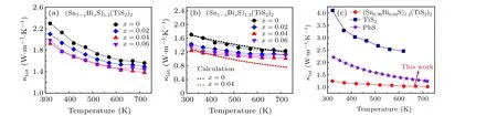
Fig. 4. Temperature-dependent (a) total thermal conductivity κtot and (b) lattice thermal conductivity κlat for (Sn1-xBixS)1.2(TiS2)2 (x =0,0.02,0.04,0.06). The black and red dashed lines correspond to the calculated temperature-dependent κlat for the pristine and x=0.04 samples using the Debye–Callaway model. (c)A κlat comparison with typical thermoelectric sulfides including TiS2[25] and PbS.[24]

Fig. 5. Temperature-dependent ZT of (Sn1-xBixS)1.2(TiS2)2 (x =0,0.02,0.04,0.06)samples. The ZT values of pristine TiS2[25] and SnS[35]are given for comparison.
Figure 5 shows the temperature-dependent dimensionless figure of merit,ZT, for the (Sn1-xBixS)1.2(TiS2)2samples (x= 0,0.02,0.04,0.06). The (Sn0.96Bi0.04S)1.2(TiS2)2exhibits higherZTvalues over the entire temperature range with a maximum reaching to 0.3 at 720 K. It is one of the highest among misfit layer compounds. The achieved performance out-performs previously reported TiS2and state-of-theart polycrystalline SnS,indicating its great potential as a lowcost thermoelectric material for power generation.
4. Conclusions
Misfit layer compounds emerge as promising low-cost thermoelectric sulfides. However, it is challenging to optimize its carrier concentration because dopants tend to form covalent bond with sulfur. We demonstrated that Bi weakly bonded with sulfur, delocalized the charge carrier and facilitated the charge transfer. Highly mobile electrons significantly enhanced electrical conductivity and power factor of(Sn0.96Bi0.04S)1.2(TiS2)2over the entire temperature range.The heavy Bi atom also exceptionally reducedκlatby introducing mass fluctuation. By virtue of the Bi doping on charge and thermal transport properties,(Sn0.96Bi0.04S)1.2(TiS2)2shows a maximumZTof 0.3 at 720 K,excelling many state-of-the-art thermoelectric sulfides including SnS and PbS.
Appendix A
Density of state mass calculation
The density of state mass(m*)is calculated according to the following equations[36,37]using the Seebeck coefficient(S)and carrier concentration(nH):

whereμis the reduced Fermi level,Fj(μ) is the Fermi integral,kBis the Boltzmann constant,his the Planck constant,andλ=0 is the scattering parameter corresponding to acoustic phonon scattering.
Lorenz number calculation
The Lorenz numberLwas obtained by single parabolic band(SPB)model with acoustic scattering(λ=0 for acoustic phonon scattering):
The disorder scattering parameterΓcalcis calculated by the model of Slack[43]and by Abeles[42]assumingΓcalc=ΓM+ΓS,whereΓMandΓSare mass fluctuations scattering parameter and strain field fluctuations scattering parameter, respectively. The mass and strain fluctuation scattering parameters are determined by[40]
Acknowledgments
This work was financially supported by the National Key Research and Development Program of China (Grant No. 2018YFA0702100), the Joint Funds of the National Natural Science Foundation of China and the Chinese Academy of Sciences’ Large-Scale Scientific Facility (Grant No. U1932106), and the Sichuan University Innovation Research Program of China(Grant No.2020SCUNL112).
猜你喜欢
赤水源(2018年6期)2018-12-06
商周刊(2017年16期)2017-10-10
女士(2017年1期)2017-03-25
今古传奇·故事版(2016年22期)2016-12-24
中共南宁市委党校学报(2016年1期)2016-10-22
少年文艺·开心阅读作文(2016年2期)2016-09-10
故事会(2015年22期)2015-11-18
小小说大世界(2014年6期)2014-06-03
故事林(2008年8期)2008-05-14
现代家庭(2000年6期)2000-06-14

- Chinese Physics B的其它文章
- A design of resonant cavity with an improved coupling-adjusting mechanism for the W-band EPR spectrometer
- Photoreflectance system based on vacuum ultraviolet laser at 177.3 nm
- Topological photonic states in gyromagnetic photonic crystals:Physics,properties,and applications
- Structure of continuous matrix product operator for transverse field Ising model: An analytic and numerical study
- Riemann–Hilbert approach and N double-pole solutions for a nonlinear Schr¨odinger-type equation
- Diffusion dynamics in branched spherical structure