
Laser-modified luminescence for optical data storage
2022-11-21 09:40XinWei魏鑫WeiweiZhao赵伟玮TingZheng郑婷Junpeng吕俊鹏XueyongYuan袁学勇andZhenhuaNi倪振华
Chinese Physics B 2022年11期
关键词:振华
Xin Wei(魏鑫), Weiwei Zhao(赵伟玮), Ting Zheng(郑婷), Junpeng L¨u(吕俊鹏),Xueyong Yuan(袁学勇), and Zhenhua Ni(倪振华)
School of Physics and Key Laboratory of MEMS of the Ministry of Education,Southeast University,Nanjing 211189,China
The yearly growing quantities of dataflow create a desired requirement for advanced data storage methods. Luminescent materials, which possess adjustable parameters such as intensity, emission center, lifetime, polarization, etc., can be used to enable multi-dimensional optical data storage (ODS) with higher capacity, longer lifetime and lower energy consumption.Multiplexed storage based on luminescent materials can be easily manipulated by lasers,and has been considered as a feasible option to break through the limits of ODS density.Substantial progresses in laser-modified luminescence based ODS have been made during the past decade. In this review,we recapitulated recent advancements in laser-modified luminescence based ODS,focusing on the defect-related regulation,nucleation,dissociation,photoreduction,ablation,etc. We conclude by discussing the current challenges in laser-modified luminescence based ODS and proposing the perspectives for future development.
Keywords: laser,luminescence,data storage
1. Introduction
The explosion of digital data is overpowering with the rapid development in artificial intelligence(AI),the internet of things(IoTs),neurotechnology advancing and so on.[1,2]Estimated by the International Data Corporation, annual volume of digital information is experiencing a substantial increase,from 33 zettabytes (ZB) in 2018 to 175 ZB in 2025.[3]Because of its higher capacity, longer lifetime and lower consumption features,the optical data storage(ODS)owns enormous potential to surpass contemporary storage technology.[4]The traditional laser modifies recording ODS such as compact discs(CDs),digital video discs(DVDs)and Blu-ray discs have exhibited highly-competitive performance of durability and energy consumption. However, due to the resolution limitation,bottlenecks of storage density emerge.[5,6]Various superresolution schemes[7–10]with complicated systems and delicate operations have been put forward,which are still advancing towards practical application. A simple strategy of information multiplexing,[11,12]allowing the storage of more dimension per location,is needed to improve the ability of ODS.
Owing to the operability of multiple physical parameters such as intensity,[13,14]emission center,[15,16]lifetime,[17,18]and polarization,[19,20]luminescent materials can be used to enable multi-dimensional ODS. Furthermore, diverse forms of luminescent materials can be accessibly fabricated. Lasermodified luminescence with high-efficiency and simple manufacturing has been considered as a classy choice to respond to the rapid increase of data storage. The precise tunability of laser irradiation allows the delicate manipulation of luminescence properties. When laser interacts with materials,processes such as reduction,[21]ablation,[22]defect-related regulation[23]and so on occur,as shown in Fig.1. The development of laser-modified luminescence will impel the application of large-scale and cost-effective ODS.
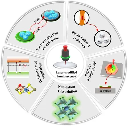
Fig. 1. Schematic diagram of laser-modified luminescence mechanism in ODS, including nucleation and dissociation, ablation, reduction, ion concentration modification, defect-related regulation (The X indicates the defect level repairment)and so on.
In this review, we overview recent achievements in data storage based on laser-modified luminescence. We first emphasize the mechanism of down-conversion luminescence(DCL) and up-conversion luminescence (UCL), respectively.Thereafter, we give a comprehensive description of DCLrelated and UCL-related luminescence modification utilized in ODS.Finally, we provide a brief discussion on the advances,challenges and opportunities of laser-modified luminescence for ODS.
2. Mechanism of luminescence
Effective regulation of luminescent process is crucial for ultrahigh density optical storage. Luminescent process is a non-equilibrium radiation thermodynamics process,[24]meaning external energy is needed to break the carrier equilibrium such as extra phonon[25]or photon.[24]Based on the difference between excitation and emission wavelength,the luminescent processes can be divided as down-conversion luminescence(DCL)and up-conversion luminescence(UCL).
2.1. Down-conversion luminescence
Converting high-energy photons to lower-energy photons,DCL process could be rendered as longer wavelength emission with shorter wavelength excitation, demonstrated via Jablonski diagram in Fig.2(a).[26]The ground,first triplet,first and second electronic states are depicted by S0, T1, S1, and S2,respectively. Conversion involving photon and electron is expressed as arrow with solid line,while electron transition without involving photon is expressed as arrow with dotted line. In the DCL processes, absorption is very crucial since the transition requires photons overcoming the energy gap between the ground state (S0) and excited state (S1or S2). As shown in the Jablonski diagram,S0electrons eventually return to the S0after undergoing a lower energy level to a higher energy level. When excited from the S0,the excited electrons tend to dissipate energy in several processes: internal conversion,fluorescence,intersystem crossing and phosphorescence. As for the internal conversion,the excited electron transits from one vibrational energy level to another level in lower electronic state, and the transition averagely occurs within 10-12s or shorter.[27]The fluorescence process is considered as a radiative process, generally happens in fluorescent material. The wavelength of fluorescence is normally longer than the excitation because of the energy loss during the internal conversion or thermal radiation. Based on the excited states difference, DCL can be divided into fluorescence and phosphorescence process, in which electrons at S1state transform to the first triplet state T1in the form of spin conversion (intersystem crossing) and phosphorescence occurs. In general, the wavelength of phosphorescence is longer than that of fluorescence. In addition,the probability of triplet emission in phosphorescence is several orders of magnitude smaller than that in fluorescence because direct transition from T1to the singlet ground state is forbidden. By using laser-induced nucleation,oxidization and etc., emission probability of fluorescence or phosphorescence can be carefully manipulated, making ODS based on DCL process achievable.
2.2. Up-conversion luminescence
Compared to DCL, UCL requires different models for further elaboration. The UCL (anti-stoke-type emission) is also known as multiphoton process,[2,28–31]during which two or more incident photons are absorbed. When excited by lower-energy light, these UCL materials can offer shorter wavelength emission, which often covert light from nearinfrared to visible range. Various mechanisms of UCL have been elaborated, including excited-state absorption (ESA),energy transfer upconversion (ETU), photon avalanche (PA),two photon absorption excitation (TPA), cooperative sensitization (CS) and cooperative luminescence (CL).[29]Among them, the ESA, ETU and PA are of higher probability of occurrence and details of which are descried as follows.
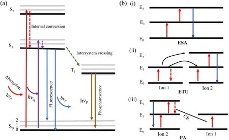
Fig. 2. (a) One form of a Jablonski diagram. (b) Energy-transfer mechanisms of UCL: (i) excited-state absorption (ESA), (ii) energy transfer upconversion(ETU),(iii)photon avalanche(PA).
(i)A typical ESA process involves ground state(E0)electron continuously absorbing pumped photons, which can be regarded as a multi-step system,as shown in Fig.2(b)(i). The electron at the E0leaps into a metastable state (E1) after absorbing photon,and then shifts from the intermediate state to a higher energy level(E2)after the absorption of another photon.The energy sum of two photons should be equal or slightly bigger than the energy of emission photon when electrons radiatively convert from E2to E0. Such process tends to occur in single ion with ladder-like arrangement of the energy levels.
(ii) ETU is a process of successive energy transfer between different adjacent ions, as shown in Fig. 2b(ii). First,the two contiguous ions in the E0absorb photons with the same energy upon irradiation and jump to E1. Rather than directly returning to the E0in the form of radiation,the energy of sensitizer ions (ion 1) transfers to the center of the activator or luminescence ions(ion 2),due to the photon absorption.Then,the electron in the re-energized ions will jump to E2and return to the E0in the form of radiation.
(iii)PA can be considered as an unconventional pumping mechanism based on a collaborative process of ESA and ETU,as shown in Fig. 2b(iii). During the PA process, the ground state(E0)is occupied in all ions,and then electron on the level E1of ion 2 can be populated by non-resonant weak groundstate absorption process. Similar to ESA,the level E2of ion 2 can be further populated. Then, an efficient cross relaxation(CR)process between the level E0of ion 1 and the level E2of ion 2 can happen,making the intermediate energy level E1occupied in both ions.And then these two ions undergo ESA,CR and interact with two another adjacent ions, resulting as four ions with E1occupation. In a similar fashion, ESA and CR will continue until E1is occupied in all ions. Eventually, the upconversion with the direct transition from level E1to level E2occurs, during which excited state absorption contains no ground state absorption.
3. ODS based on DCL
3.1. Defect-related regulation
Defects commonly exist in luminescent materials such as persistent luminescent materials(PSLM),two-dimensional transition metal dichalcogenides (TMDCs), etc. The laser–defect interaction will highly affect the charge carrier trapping and de-trapping in luminescent materials. These defectrelated luminescent materials have been widely employed in lighting,[32,33]biological fields[34,35]and ODS.[36]The laserbased defect regulation results in various luminescence manifestations, leading to marvelous applications of defect–laser interaction based ODS.
As a particular member in the advanced optical materials,[2,37,38]PSLM can store charge carriers produced by high energy photon through various defect trapping, and create light emission during the high-temperature thermal stimulation or photoexcitation process.Hence,the PSLM have been widely applied invivobio-imaging,[39,40]light-emitting diode alternating,[41,42]security signs for dark conditions[43]and so on. Benefited from the excellent erasable–rewritable ability based on repeatable photons releasing process, PSLM have been recognized as a possible rewritable data storage candidate once the following engineering roadblocks are overcome.Firstly, for bit-by-bit optical data write-in and readout, light–matter interaction on the micrometer scale is needed. Secondly,for increasing the probability of charge carrier trapping and de-trapping at room temperature, materials with appropriate trap depth are required.[2,44]A large number of groups have made great effort overcoming the above issues. Qiuet al.demonstrated that calcium aluminosilicate glasses doped with Ce3+, Tb3+, and Pr3+can emit bright and long-lasting phosphorescence covering blue, green, and red light range, after irradiated by a 800 nm femtosecond (fs) pulsed laser, as shown in Fig. 3(a).[45]Attributed to the recombination of holes and trapped electrons induced by the laser irradiation,such work paved a new way for ODS and three-dimensional image displaying in transparent matrix.[46,47]Zhuanget al.presented that various patterns (QR code, building sketch and etc.) can be rewritten in persistent luminescence film((Sr1-xBax) Si2O2N2: Eu/Yb, Dy) by 405 nm laser irradiation, and the read-out is via optical microscope after thermal annealing or 980 nm laser scanning,as shown in Fig.3(b).[48]Due to the adjustable emission, the ODS can be expanded to emission-intensity-multiplexing or emission-wavelengthmultiplexing. Linet al.extended PSLM based ODS to bulk glasses (LiGa5O8: Mn2+nanocrystals).[49]By focusing 405 nm lasers into the glass at different depths,miscellaneous patterns were realized. After exposed to ultraviolet light, the bit-by-bit data readout can be archived by 808 nm NIR laser scanning, as shown in Fig. 3(c). It is remarkable that the intensity and wavelength can still be regulated by ultraviolet radiation or heat treatment time,even after laser writing,which can highly improve the information dimension of ODS.
Luminescence of TMDCs with excitons (X0), trions (X-/X+) and biexcitons (XX) can be regulated by laser repairing or passivating of the existent defects, making the TMDCs promising defect related ODS candidates.[36,50–53]For example, Zhaoet al.demonstrated that PL enhancement could be easily achieved in exfoliated monolayer WS2under low-power laser irradiation, because oxygen attachment played a significant role in curing sulfur vacancy (VS).[51]Moreover, Sivaramet al.demonstrated that H2O molecules can overcome a large adsorption barrier with the assistance of photogenerated excitons to passivate VSin the chemical vapor deposition grown MoS2,resulting in a 200-fold increase in PL intensity.[53]Zhaoet al.focused on the PL intensity change in ozone treated WS2before and after laser irradiation,and developed defect-related TMDCs ODS,as shown in Fig.3(d).[36]They controlled fluorescence contrast by introducing localized unoccupied states via ozone irradiation, then used focused laser beam scanning to passivate defects via substitution of the VSwith oxygen atoms. By defect curing, an erasable,high resolution and atomic thin disk was achieved. The use of low-dimensional materials will benefit the extending of highdensity ODS to low-dimensional regime,along with effective encryption of information storage.
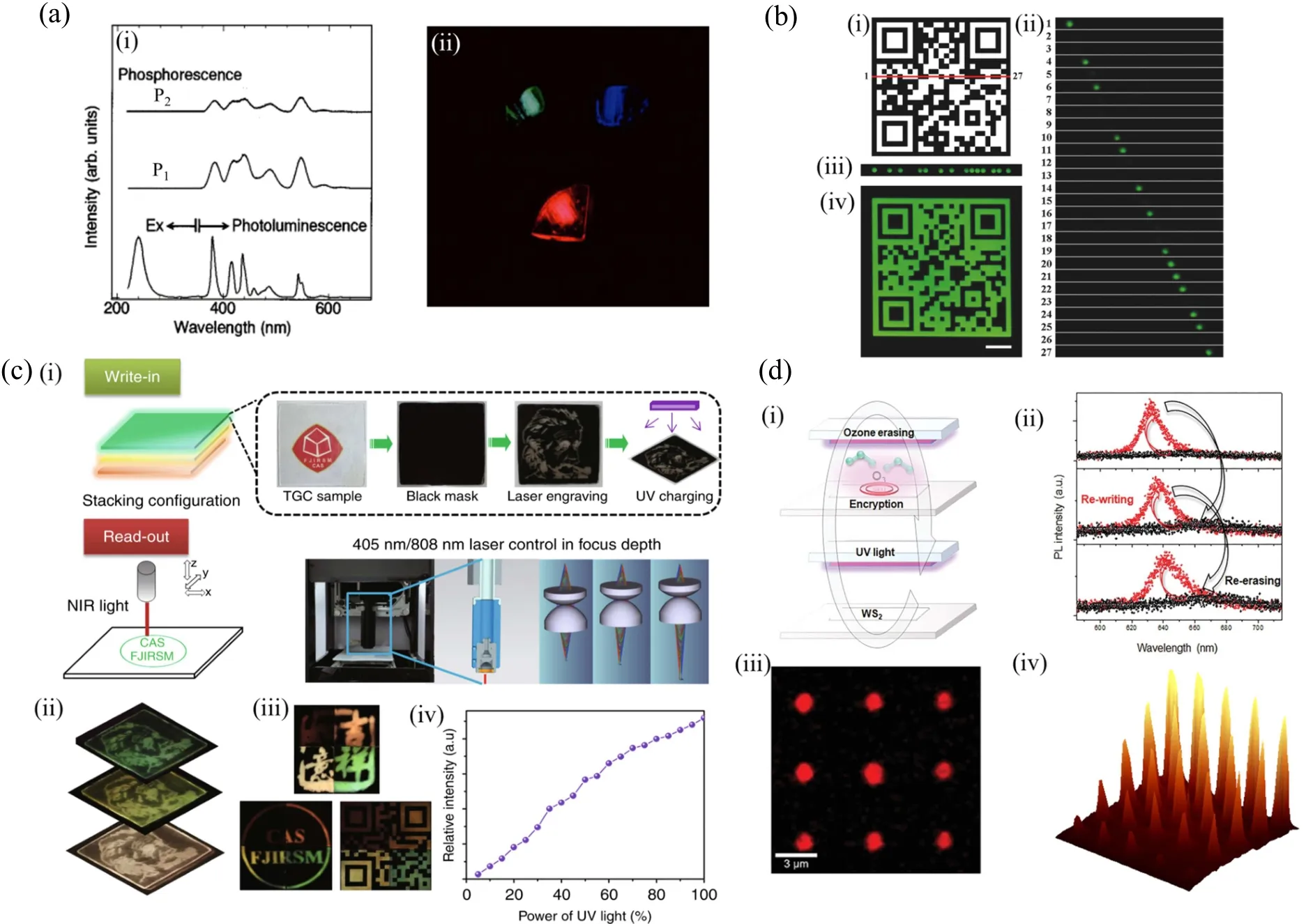
Fig.3. Defect-related regulation based data storage. (a)The photoluminescence of Ln2+-doped glass. The P1 and P2 are phosphorescence spectra of the glass after the laser irradiation of 350 s and 1000 s,as shown in(i). The Ce3+,Tb3+ and Pr3+-doped calcium aluminosilicate glass sample presents blue, green and red-light emission, respectively, as shown in (ii).[45] (b) The QR code patten written demonstration was shown in film SSON:Eu, irradiated by a 405 nm laser. (i) Pre-set QR code pattern for data storage. (ii) After laser write-in, a 980 nm laser was used to read out information at different positions along the red line shown in (i), which showed green luminous spot. (iii) A summary image by managing 27 graphs in(ii). (iv)Photograph rather than bit by bit readout of the QR code by heating. Scale bar: 5 mm.[48] (c)Illustration of the multilayer information write-in/readout process in transparent LiGa5O8: Mn2+ glass. (i) The bit-by-bit mode was done via 405 nm and 808 nm NIR laser scanning progressively. (ii) High quality 3D optical readout in different layers with heat assistance. (iii) Wavelength modulated by controlling the heating time. (iv) The intensity multiplexing could be controlled by varying the input UV irradiation power.[49] (d) Illustration of the cyclic on-WS2 rewriting process based low dimensional ODS.(i)Schematic of multiple cycles. (ii)Red and black spectra corresponding to write-in and ozone erasing,respectively. (iii)An array diagram of recording points. (iv)The intensity of the exciton peak can be precisely controlled by writing power.[36] Panels(a)–(d)were reproduced from Refs.[36,45,48,49],respectively,with permission.
3.2. Nucleation and dissociation
Forming direct band gap or luminescent center by nucleation is a key step for luminescent materials-based ODS.Nucleation is a self-organizing process, during which barrier energy is broken through and novel thermodynamic phase or self-assembled structure emerges.[54,55]Various methods for nucleation fabrication have been proposed, such as sol–gel technique,[56,57]hydrolysis method,[58,59]CVD,[59,60]laser heating treatment[61–63]and so on. Among them, laser heating treatment is particular suitable for ODS due to its highresolution, efficiency and controllability. Predominant influence for laser heating based nucleation treatment is attributed to three key parameters: location,irradiation duration and energy density.[64]For instance, Linet al.presented the synthesis of CdSe and core-shell CdSe/CdS QDs via 532 nm laser irradiation for 3 hours, production of which can be effectively used in ODS.[65,66]Arciniegaset al.reported that CH3NH3PbI3microcrystals (~50 μm) and nanocuboids (~500 nm)can be controllably produced by tuning the laser parameters (power density or irradiation time).[67]Zhanet al.demonstrated thatγ-CsPbI3QDs with a high quantum yield(92%) can be achieved by removing solvent DMF with the accumulation of heat induced by 405 nm laser.[68]By manipulating laser direct writing parameters, patterns with scalable resolution can be manufactured, as shown in Fig. 4(a).Vetchinnikovet al.demonstrated that laser-induced temperature gradient can lead to the formation of CbS QDs in CdSdoped silicate glass.[69]In addition, thein-situfabrication or decomposition of QDs respectively only requires fs laser pulse number of 103and 106, paving new solution for repeatable and reversible writing of optical storage information,as shown in Fig. 4(b). Recently, the reversible 3D laser-induced nucleation and dissociation of CsPbBr3QDs have been demonstrated by Huanget al., which was realized via fs-800 nm working platform, as shown in Fig. 4(c).[70]When the pulse laser is focused into the transparent glass, the glass absorbs photon energy through nonlinear effect due to the ultra-high peak power. The temperature of the focused area exceeds the glass transition temperature, and the atoms (Cs, Pb, S) at the center of laser irradiation area moves and aggregates to form crystal nuclei (~1 nm). As crystal seeds, these cores grow and form perovskite QDs after subsequent lower temperature heat treatment. Hence, the presupposed information can be stored in the glasses after nucleation treatment. In particular, further fs laser irradiation can erase the recorded information in CsPbBr3QDs, but the information can be repeatably recovered through annealing process, suggesting repetitive and stable ODS capability. Huanget al.also demonstrated that information based on blue PL can be recorded,erased and then recovered in glasses by controlling the formation of CsPb(Cl/Br)3QDs.[71]Sunet al.presented the 3D direct laser writing of tunable composition and band gap perovskite nanocrystals(CsPb(Br1-xIx)3)using fs lasers.[72]The PL wavelength ranged from 520 nm to 690 nm,offering a new dimension for ODS, as shown in Fig. 4(d). By tuning irradiation time, ultrafast laser can induce liquid nanophase separation, leading to ion exchange between Br-(smaller radius)and I-(larger radius). The recorded information possessed high-temperature stability,which can be of potential for ODS with high stability.

Fig.4. Nucleation based ODS.(a)In situ direct laser writing fabrication of patterned dots lines and pattern,based on γ-CsPbI3 QDs.[68](b)Optical(i)and luminescence(ii)microscope images of the domains array laser-written in CdS-doped glass(λexc.=330–385 nm).[69](c)(i)Optical images(upper) and readout signal intensity mapping images (lower) of CsPbBr3 quantum dots array under UV light. (ii) The relationship between PL intensity,peak wavelength and full-width at half-maximum(FWHM)and number of cycles of the CsPbBr3 quantum region during erasure recovery.Scale bars: 100 μm.[70] (d)(i)Schematic diagram of direct lithography of composition-tunable perovskite CsPb(Br1-xIx)3 nanocrystals(NCs)in glass. (ii)PL spectra of NCs with different composition. (iii)Photograph(top)and PL mappings(bottom)of CsPb(Br1-xIx)3 NCs. The scale bar is 10 μm,and the excitation wavelength is 405 nm.[72] Panels(a)–(d)were reproduced from Refs.[68–70,72],respectively,with permission.
3.3. Photoreduction
Photoreduction is the process of chemical reduction under light irradiation, often associated with the formation of fluorescence emission center, and is widely used in ODG.Compared with continuous-wave laser, fs laser is adapted to photoreduction because large number of free electrons can be induced by multi-photon ionization,[73,74]tunneling ionization[75,76]and avalanche ionization[77,78]at the focused area. Chenet al.presented that laser-induced Te4+reduction and Te2molecular clusters forming(with NIR luminescence)could be effectively controlled via fs laser irradiation.[79]Penget al.found that Bi3+can be reduced to Bi+after fs laser irradiation and exhibited NIR PL under 785 nm laser diode pumping.[80]Watanabeet al.presented valence state of silver(Ag)ion modification in Ag2+-doped soda-aluminophosphate glass using intense near-UV fs laser irradiation.[81]Bellecet al.demonstrated that Ag+transformed to Ag atoms(Ag0)and then to Agx+m(m: the number of atoms,x: the ionization degree)by using a high repetition rate infrared fs laser,which involved different physical mechanisms at different time scales, as shown in Fig. 5(a).[82]A nonlinear 4-photonabsorption occurred instantaneously,and the Ag+trapped the electrons after photoelectron transformation. Then, the Ag0was trapped by the Ag+ions to form silver clusters Agx+m(m <10), which exhibited strong fluorescence under 405 nm irradiation. Employing silver clusters as storage medium,Royonet al.showed the fs-laser modified Ag2+-doped glasses could be used for ODG,as presented in Fig.5(b).[83]The fluorescence grayscale was regulated linearly when tuning the number of pulses, and optical information containing various portraits was explicitly recorded in different depths without information cross talk. Miuraet al.created a multilayer,rewriteable and high signal-to-noise ratio (PL contrast) data storage in samarium(Sm)ions doped glass,based on the photoreduction and photo-oxidation of Sm ions.[84]The PL emission (~680 nm) sub-micron-size of the laser-irradiated area obtained in their work is shown in Fig. 5(c), suggesting the size limitation breakthrough ability. Hereafter, Riesenet al.demonstrated that the PL induced by d–f (Sm2+:5D0→7F0)transitions was suitable for low power read-out. The Sm2+5D1→7FJluminescence emerged when the read-out power increased, which may influence the signal-to-noise ratio.[85]Recently, Wanget al.studied the photoreduction of Sm3+to Sm2+induced by fs-laser one-pulse irradiation in Sm3+-doped sodium aluminoborate glass, which could increase the speed of information writing.[86]Both the PL intensity and diameter of data recording dots could be controlled regularly by tuning the pulse duration and energy, as shown in Fig.5(d), proving that the photoreduction reduction based ODS could be subtlety controlled. Furthermore, the single-shot photon information recording in glass has been successively achieved, which can be of great potential for large capacity ODS.

Fig. 5. Photoreduction based ODS. (a) Schematic view of the Agx+m nanostructures formation is shown as (i). Fluorescence microscopy and corresponding HRSEM images showed a cross pattern was created by moving the sample first in the x direction and then in the y direction, as shown in(ii).[82] (b)Writing and reading experimental setups and fluorescence grayscale encoding in Ag2+-doped glass. Recorded images viewed by confocal fluorescence microscopy and side view of the recorded images(λexc. =405 nm)of three French Nobel laureates in physics: Gabriel Lippmann, Alfred Kastler, and Claude Cohen-Tannoudji, as in (ii).[83] (c) The difference of photoluminescence spectra obtained by excitation at 488 nm for a laser irradiated area or not in the interior of the Sm3+-doped glass(i). Signal readout by detecting the fluorescence for photoreduction bits with a 200 nm diam(ii).[84] (d)PL intensity and diameter of emissive dots as a function of pulse duration and energy in Sm3+-doped glass.[86]Panels(a)–(d)were reproduced from Refs.[82–84,86],respectively,with permission.
3.4. Photoinduced ablation and others
The interaction between laser and matter is affected by many factors, such as the pulse width, power density, wavelength.In fact,all these laser-interacted materials with fluorescence contrast are of potential to be new storage strategies for fluorescence-based ODS. In addition to methods mentioned above, experimental studies on laser-induced ablation,[87,88]two-photon absorption photo-bleaching,[89,90]laser-induced fluorophores[91]have also been employed to achieve high density ODS. For instance, Luet al.demonstrated that the pattern and thickness of MoS2sheets could be precisely controlled with a focused laser beam,resulting in layer-dependent band gap engineering.[87]Zhouet al.optimized the thickness of(FAPb(BrxI1-x)3)nanoplatelets modification using fs laser and modulated the fluorescent emission from red (690 nm)to green (540–600 nm), as shown in Fig. 6(a).[92]Based on fs-DLW system, in the form of holes, laser ablation enabled microscale-resolved multicolor emission and color adjustable ability with the nanoplatelet thickness manipulation.Chenet al.presented that thermoplastic polyurethane with outstanding mechanical properties displayed fluorescence intensity linearly dependent on the pulse energy by harnessing fs laser. The encoded multilayer information remains high readout accuracy after multiple bending cycles,indicating that the thermoplastic polyurethane is of potential to be densely rolled up.[91]Weiet al.reported that data storage with ultrahigh capacity based on fs laser induced PL in low-cost plastics, including polycarbonate (PC), precipitated calcium carbonate(PCC),polystyrene(PS),and polymethyl methacrylate(PMMA).[93]The data storage can be realized via controlling single pulse using high-frequency electro-optic modulator(EOM).Multiple gray levels and 100 layers on both sides of a standard disc can be assigned by adjusting the power density and focus position of the focused laser,as shown in Fig.6(b).Thermally stable penta-functional monomer dipentaerythritol pentaacrylate developed by Gaoet al.improved the ODS data lifetime to nearly 250 years at ambient environment.[12]Yuanet al.embedded aggregation-induced emission material(fluorescent molecule tetraphenylethene (TPE)) into the tape by soaking in TPE powder solution for long time.[90]The twophoton absorption photo-bleaching effect occurred,leading to irreversibly destroying of the excited state molecules of TPE under 515 nm fs laser. Six-layer information recording inside the transparent tape was realized, as shown in Fig. 6(c), providing a new method to adopt fluorescent molecule into high density ODS.
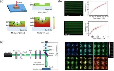
Fig. 6. Photoinduced ablation based ODS and others. (a) Scheme of the direct laser writing on high-quality halide-mixed formamidinium lead mixed-halide (FAPb(BrxI1-x)3) NP with different thickness (~50 nm, ~200 nm, 500–1000 nm).[92] (b) ODS written by a fs laser with a single pulse in PMMA and its relative pulse energy evolution of the dots (1st and 50th layers). Scale bar: 20 μm.[93] (c) Optical set-up used for recording data points inside fluorescent molecule tetraphenylethene-dipped transparent. The readout result presented six recording layers under two-photon illumination in the photobleaching transparent fluorescent tape.[90] Panels(a)–(c)were reproduced from Refs.[90,92,93],respectively,with permission.
4. ODS based on UCL
With the high penetration depth, low damage to biological samples, narrow emission bands, adaptability for storage,etc., UCL have been applied in various applications.[94–96]Lanthanide ions (Ln3+) such as Yb3+/Er3+and Yb3+/Tm3+shown in Fig.7(a)exhibit general form of 5s25p64fn,producing wavelength manipulable UCL emission.[96,97]The unique UCL of Ln3+is related to the electrons transition between 4f energy levels,[98]which can be functionalized for ODS.For instance, Zhanget al.reported thatβ-NaYF4: Yb, Er with UCL characteristic under near-IR excitation was overlapped with photochromic diarylethene, and the ETU process could be used for emission tuning. Rewritable ODS and nondestructive readout can then be archived with the assistance of single-beam irradiation.[99]Baiet al.provided a novel tactic for ODS based on reversible modification of UCL in photochromic ceramic (PbWO4:Yb3+, Er3+), as shown in Fig.6(b).[100]Tuning the duration time of 532 nm irradiation,the Pb2++hν →Pb4++2e-and W6++e-+hν →W5+reactions can be controlled to influence the photochromic degree,UCL modified degree of which was regulated up to~80%.
High density ODS requires efficient use of bulk space,making UCL inside transparent materials be particularly important. Wanget al.completed abundant multicolor luminescent patterns in a plate based on UCL,using Er:Cs3YbF6NCs@ glass inks.[101]Tenget al.also presented ODS inside the transparent rare earth ion(Er3+)imbedded glasses,with emission located at 525 nm and 545 nm.[102]Huanget al.proposed that UCL in Dy3+-doped glass could be regulated by optimizing the fs laser spectral phase.[103]Xiaoet al.confirmed that ODS in rare earth ions(Yb3+,Er3+,Tb3+)doped transparent glasses (Sb and W elements contained) glass could be realized based on UCL,as shown in Fig.6(c).[104]The UCL was ascribed to ETU process between two rare earth ions before the radiative transition from2H11/2,4S3/2and4F9/2state to ground state of Er3+,respectively. The high peak power of fs laser promoted multiphoton absorption, resulting in the reactions of Sb3++hν →Sb5++2e-and 2W6++hν+2e-→2W5+after 800-nm fs laser irradiation. In summary,the UCL overcomes the overlapping between the UCL and excitation laser, and presents huge potential of archiving nondestructive information reading out.
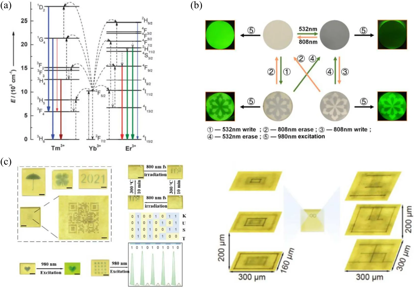
Fig. 7. Modified UCL based ODS. (a) Energy transfer mechanisms showing the UCL processes in Er3+, Tm3+, and Yb3+ doped crystals under 980-nm diode laser excitation. The dashed-dotted, dashed, dotted, and full arrows represent photon excitation, energy transfer, multi-phonon relaxation, and emission processes, respectively. Only visible and NIR emissions are shown here.[96] (b) Reversible writing and erasing of the flower pattern of PbWO4:Yb3+, Er3+ ceramic by alternating 532 nm irradiation (600 mW/cm2, 40 s) and 808 nm irradiation (2.5 mW/cm2,140 s).[100](c)Photochromic pattern information,digital information,and raw and enlarged photochromic 2D code pattern and information readout by 980 nm irradiation. 3D pattern in the interior of Ln2+-doped glasses with different sizes and Chinese characters “three”, “four”, and “five”recorded in various layers of the glass.[104] Panels(a)–(c)were reproduced from Refs.[96,100,104],respectively,with permission.
5. Conclusion and perspectives
Laser modified luminescence based ODS owns enormous potential in this era of information explosion.In this review we have shown the potential of laser-modified luminescent materials for optical data storage: higher capacity, longer lifetime and lower energy consumption features compare to the current mainstream solid state disk drive technique. The mechanisms of luminescence are generally elaborated for the purpose of more effectively regulating of luminescence. We give a description how laser is utilized to ODS via various physical or chemical interactions such as laser induced defect-related regulation, nucleation and dissociation, photoreduction, ablation and other conditions. Based on mechanisms of laser modified luminescence,we give detailed introductions of development of various laser modified luminescence based ODS and the benchmark parameters for these materials are listed in Table 1. Table 1 summarizes the state of the art of laser modified luminescence based ODS:various materials have been proven efficient candidate for laser modified ODS and storage density in LiGa5O8:Mn2+(~16.25 TB·cm-3)even exceeds currently widely-used solid state disk drive technique.
Though decent progresses have been made,there are still considerable challenges and features to meet the demanding requirement of data storage in the future.
Storage density Storage density,as the most critical technical indicator of capacity,should be substantially improved in order to deal with mass data generated in the future. However,the maximum storage density under current theoretical framework is approaching theoretical limit of storage density even with a high N.A.objective.[105]Hence,novel mechanisms and methods out of the box should be employed to break the conventional storage capacity limit of OSD.
Data throughputs A followed challenge in front of big data storage is fast writing and reading throughputs. The writing and reading processes of laser modified ODS strongly depend on the number of laser pulses. However, the laser frequency and parallel quantities of laser spots in current technique need to be precisely controlled (to efficiently write in information without introducing unnecessarily damage)to obtain high throughputs in different materials, which in turn greatly limit the application of big data storage in the future.Therefore,boosting throughputs is another important issue.
Data security and lifetime Information security has become a major issue. As one promising candidate of data storage method in the future, it would be desirable to realize an ODS platform for future demand of ultrahigh-security storage. Besides, developments of storage device with ultralong lifetimes put forward new challenges on laser modified luminescence based ODS.

Table 1. Representative characteristics of ODS based on luminescence. The storage density was calculated and analyzed based on experimental results presented in individual work from each groups.
In view of the above issues, several strategies have been proposed, such as decreasing laser focal area or increasing storage dimensions in ODS. To some content, these methods improve corresponding properties,but most of these methods have not met the best expectations. Therefore,tremendous efforts should be paid in the following points to overcome the obstacles listed before.
1. Deepen the understanding of interaction between ultrafast fs laser and materials. The dynamic interaction process (linear effect, near-field processing)between fs pulse laser and materials is not wellunderstood yet, where some explanations are of much controversial.[106,107]Super-resolution processing, an approach breaking the diffraction barrier could be realized with better understanding of physical origin of laser-modified luminescence,[108]thus ultrahigh capacity will be achieved with greatly enhanced storage density and higher dimension storage. Furthermore, it would be very helpful to propose effective optical parallelism methods for generating multi-arrays lasers shots to boost writing and readout in large scale.[109]
2. Performing as sole input, the light itself, which possesses rich dimensional features, can be synergistically used in multi-dimensional information storage and encryption system. Separately or synergistically combining more than six-dimensional features of the input light(wavelength,duration,phase,polarization,depth,power and etc.),information could be efficiently encrypted into one storage material.[30]With specific input features thrown into a magic box, complete information can be read out only when the box matches well with the added features. According input light feature demand,suitable materials with special structures could be purposefully designed and prepared, with the capacity of outputting the predesigned encryption under corresponding input.
3. Introduction of novel materials and novel structures.Many new nanomaterials emerge with the development of nanotechnology. Several types of nanomaterials are believed to be promising candidates for the next-generation ODS, such as metallic nanoparticles, 2D materials, semiconductor quantum dots and rare-earth-doped nanocrystals. For example, recently extensively-studied monolayer transition metal dichalcogenides (TMDCs) could be an excellent platform for ODS.First of all,the nature of ultrathin thickness (atom scale) ensures a maximum storage density, which is the top challenge for big data storage.Second, quantum confinement and valley-contrasting physics turn emitters in TMDCs into entangled singlephoton sources.[110–114]As a main role in quantum information scheme, data equipped with quantum characteristics will be unconditionally secure when quantum encryption is employed.[115]With laser-modified method, high-quality quantum emitters would be fabricated in larger scale and with high-yield.[116,117]Besides, recent progress of TMDCs on twistroincs endows the emitted photons with more degree of freedom, in which excitonic photons can be fancy complex information carriers.[118–123]Lastly, combination with novel structures, such as metasurfaces, would be another direction to realize the laser modified luminescence based ODS for the future. Known as a planar version of artificial materials, metasurfaces enable possibilities to manipulate light through multi-degree of freedom, which is highly beneficial to high density and multi-function of ODS.[124]Moreover, the success of optical holography using metasurfaces made by metal,dielectrics and 2Ds has proven the high potential on chip-integration.[125–129]Therefore, we believe metasurfaces would be another methods boost the function of ODS for future.
Acknowledgement
Project supported by the National Natural Science Foundation of China(Grant Nos.61774034 and 12104090)
猜你喜欢
汽车实用技术(2022年14期)2022-07-30
新课程(2022年25期)2022-07-14
中国典型病例大全(2022年7期)2022-04-22
故事林(2020年17期)2020-10-09
山东农业大学学报(自然科学版)(2020年3期)2020-07-15
雷锋(2020年5期)2020-06-12
北京广播电视报(2019年21期)2019-09-02
当代工人(2016年23期)2017-02-27
天池小小说(2009年7期)2009-08-06

- Chinese Physics B的其它文章
- A design of resonant cavity with an improved coupling-adjusting mechanism for the W-band EPR spectrometer
- Photoreflectance system based on vacuum ultraviolet laser at 177.3 nm
- Topological photonic states in gyromagnetic photonic crystals:Physics,properties,and applications
- Structure of continuous matrix product operator for transverse field Ising model: An analytic and numerical study
- Riemann–Hilbert approach and N double-pole solutions for a nonlinear Schr¨odinger-type equation
- Diffusion dynamics in branched spherical structure