
Sputtered SnO2 as an interlayer for efficient semitransparent perovskite solar cells
2022-11-21 09:40ZhengFang方正LiuYang杨柳YongbinJin靳永斌KaikaiLiu刘凯凯HuipingFeng酆辉平BingruDeng邓冰如LingfangZheng郑玲芳ChangcaiCui崔长彩ChengboTian田成波LiqiangXie谢立强XipengXu徐西鹏andZhanhuaWei魏展画
Chinese Physics B 2022年11期
Zheng Fang(方正) Liu Yang(杨柳) Yongbin Jin(靳永斌) Kaikai Liu(刘凯凯) Huiping Feng(酆辉平)Bingru Deng(邓冰如) Lingfang Zheng(郑玲芳) Changcai Cui(崔长彩) Chengbo Tian(田成波)Liqiang Xie(谢立强) Xipeng Xu(徐西鹏) and Zhanhua Wei(魏展画)
1MOE Engineering Research Center for Brittle Materials Machining,Institute of Manufacturing Engineering,College of Mechanical Engineering and Automation,Huaqiao University,Xiamen 361021,China
2Xiamen Key Laboratory of Optoelectronic Materials and Advanced Manufacturing,Institute of Luminescent Materials and Information Displays,College of Materials Science and Engineering,Huaqiao University,Xiamen 361021,China
SnO2 is widely used as the electron transport layer(ETL)in perovskite solar cells(PSCs)due to its excellent electron mobility, low processing temperature, and low cost. And the most common way of preparing the SnO2 ETL is spincoating using the corresponding colloid solution. However, the spin-coated SnO2 layer is sometimes not so compact and contains pinholes,weakening the hole blocking capability. Here,a SnO2 thin film prepared through magnetron-sputtering was inserted between ITO and the spin-coated SnO2 acted as an interlayer. This strategy can combine the advantages of efficient electron extraction and hole blocking due to the high compactness of the sputtered film and the excellent electronic property of the spin-coated SnO2. Therefore,the recombination of photo-generated carriers at the interface is significantly reduced. As a result,the semitransparent perovskite solar cells(with a bandgap of 1.73 eV)based on this double-layered SnO2 demonstrate a maximum efficiency of 17.7%(stabilized at 17.04%)with negligible hysteresis. Moreover, the shelf stability of the device is also significantly improved,maintaining 95%of the initial efficiency after 800-hours of aging.
Keywords: semitransparent perovskite solar cells,sputtering,interlayer,hole blocking
1. Introduction
Perovskite solar cells (PSCs) have achieved unprecedented power conversion efficiency(PCE)growth from 3.8%in 2009 to the current 25.7%.[1–8]The SnO2electron transport layer (ETL) has played a crucial role in improving the PCE of PSCs in the past few years. Due to the favorable properties such as large bandgap,better energy level alignment,high electron mobility, and good stability under ultraviolet (UV)light,SnO2has become a widely used ETL.[9–15]These properties make the SnO2-based PSCs exhibit more efficient light harvest, enhanced electron extraction, suppressed hysteresis,and improved UV stability.[16–18]
Many methods have been developed for fabricating the uniform SnO2thin films, including solution spin-coating,[10]electrodeposition,[19]sputtering,[20]chemical bath deposition(CBD),[21]and atomic layer deposition (ALD).[22]Among them,spin-coating using SnO2nanocrystal precursor is widely used due to its high device efficiency, low hysteresis, low processing temperature,and good cost-effectiveness.[13]However,the spin-coated SnO2thin films frequently contain some undesired pinholes,which lead to direct contact between perovskite film and the ITO electrode, resulting in the recombination of carriers. Uniform and compact SnO2film can be obtained by magnetron sputtering, but the electron mobility and the device performance are not as good as that obtained by spin-coating.[20,23,24]The preparation of SnO2by ALD can accurately control the film thickness, which is suitable for large-area film preparation with good uniformity. However,the resultant device performance can not compete with the spin-coating one, and the cost of ALD is expensive.[22,25,26]Besides,CBD is suitable for large-area manufacturing,but the preparation process is complex.[7,21]
To improve the quality of SnO2film by utilizing the existing facile fabrication methods, researchers have developed the double-layered ETL strategy.[27]For example, doublelayered ETLs with SnO2/fullerene (C60) or fullerene derivatives (PCBM) have been demonstrated. It was found that C60/PCBM can repair the defect of the SnO2film and suppress the charge recombination.[28,29]Junget al.designed a bilayer structure of SnO2/ZnO, which can effectively suppress the trap-assisted recombination in the interface between ETLs and PSCs.[30]Songet al.demonstrate a double-layered SnO2/NH4Cl-SnO2as an efficient ETL,which shows a better energy level alignment with the perovskite and enhanced electron extraction efficiency.[31]The double-layered ETL strategy can effectively overcome the pinhole issue of the spin-coated film because the additional layer can fill the formed pinholes.
As an alternative approach, here we develop a composite ETL by magnetron sputtering a SnO2interlayer(SP-SnO2)between ITO and the subsequently spin-coated SnO2film(SC-SnO2)to fabricate high-performance semitransparent perovskite solar cells (ST-PSCs). The SP-SnO2layer can effectively increase the film compactness and the blocking ability of the photo-generated holes, while the SC-SnO2enables efficient electrontransporting properties. This approach makes the composite ETL combine the advantages of sputtering and spin-coating. As a result, the ST-PSCs based on an optimized SP-SnO2thickness of~12 nm exhibited significantly increased open-circuit voltage (VOC) and fill factor (FF) and achieved a PCE of 17.7%with negligible hysteresis. In addition,the sputtered interlayer also improved the device’s stability. The device with SP-SnO2interlayer maintained 95% of the initial PCE after being stored for over 800 hours.
2. Experimental details
2.1. Materials
Materials in experiments include tin (IV) oxide (SnO2,15% in H2O colloidal dispersion, Alfa Aesar), tin (IV) oxide target materials (ZhongNuo Advanced Material Technology Co., LTD), lead iodide (PbI2, 99.99%, TCI), formamidinium iodide (FAI, 99.99%, GreatcellSolar), methylamonium iodide (MAI, 98.0%, TCI), methylammonium chloride(MACl, 98.0%, TCI), 2,2′,7,7′-tetrakis (N,N-p-dimethoxyphenylamino)-9,9′-spirobifluorene (Spiro-OMeTAD, Sigma-Aldrich), lithium bis (trifluoromethanesulfonyl)imide (Li-TFSI, 99.95%, Sigma-Aldrich), N,N-dimethylformamide(DMF, 99.8%, Sigma-Aldrich), dimethyl sulfoxide (DMSO,99.9%, Sigma-Aldrich), isopropanol (IPA, 99.8%, Sigma-Aldrich), chlorobenzene (99.9%, Sigma-Aldrich), 4-tertbutylpyridine (4-TBP, 96%, Sigma-Aldrich), molybdenum(VI) oxide (MoO3, 99.97%, Lumtec), ITO targets (90 wt%In2O3, 10 wt% SnO2, ZhongNuo Advanced Material Technology Co.,LTD).All materials were used as received without further purification.
2.2. Solution preparation
The SnO2nanocrystal solution was obtained by diluting the SnO2colloidal solution with deionized water (v/v=1:2). The PbI2precursor solution was prepared by dissolving 437.0 mg of PbI2, 348.7 mg of PbBr2, and 24.7 mg of CsI in 1 mL mixed solvent of DMF and DMSO (v/v= 9 : 1).The organic salts solution was prepared by dissolving 67.4 mg of FAI, 25.8 mg of MAI, and 28.5 mg of MACl in 1 mL of IPA.The HTM solution was obtained by dissolving 90 mg of Spiro-OMeTAD in 1 mL of chlorobenzene with the addition of 36.1 μL of 4-TBP and 21.8 μL of Li-TFSI(520 mg·mL-1in acetonitrile).
2.3. Fabrication of ST-PSC
The patterned indium tin oxide (ITO) substrates were sequentially cleaned with water, acetone, isopropanol, and ethanol under sonication for 20 min,respectively.A thin SnO2film with different thicknesses (~6 nm, 12 nm, and 18 nm)was deposited by a sputtering system (Shen Yang Ke Cheng VacuumTechnology Co., LTD) at room temperature to form the first SnO2layer. SnO2target was used for the deposition,and pure oxygen was used as the reactive gas. The chamber for the sputtering process was first evacuated to a base pressure of below 5×10⁻⁴Pa before sputtering. During the sputtering process, the deposition rate was 0.1 ˚A/s, and the cavity pressure was maintained at 0.15–0.2 Pa. After that,the substrates were treated with plasma treatment for 5 min. The diluted SnO2nanocrystal solution was spin-coated on the substrate at 4000 rpm for 30 s and followed by annealing on a hotplate at 150°C for 15 min in the air to form the second SnO2layer.
The perovskite films were obtained through the two-step sequential deposition process in a glove box with an N2atmosphere. For the first step,the PbI2precursor solution was spincoated on SnO2substrates at 2000 rpm for 30 s, followed by an annealing process at 70°C for 1 min in the N2atmosphere.For the second step,the organic salts solution was spin-coated on the PbI2-coated substrates at 1700 rpm for 30 s and annealed in the air(the relative humidity is 10%–20%)at 150°C for 15 min. The hole-transport layer was deposited on the perovskite film by spin-coating the HTM solution at 3000 rpm for 30 s. For the front transparent electrode, a 20 nm thick MoOxbuffer layer was thermally evaporated on the substrate in a vacuum chamber (5×10⁻⁴Pa), and the deposition rate was 0.5 ˚A/s. Then the ITO transparent electrode was formed by magnetron sputtering of 200 nm ITO using RF magnetron sputtering at 70°C.During the film deposition,the RF power was 50 W,the deposition rate was 0.5 ˚A/s,and the cavity pressure was maintained at 0.15–0.16 Pa. Finally,a patterned Ag electrode with a thickness of 70 nm was thermally evaporated on the edge of the device to improve the conductivity of the electrode.
2.4. Characterization
Scanning electron microscopy (SEM) was carried out on a field-emission scanning electron microscope (JEOL JSM-7610F).Ultraviolet-visible(UV-vis)transmittance spectroscopy and steady-state photoluminescence (PL) spectra of perovskite films were acquired on an instrument supplied by Xipu electronics equipped with an integration sphere in the glovebox. Time-resolved photoluminescence (TRPL) was measured by the FLS920(Edinburgh Instruments Ltd)with a pulsed excitation at 375 nm.Electrochemical impedance spectroscopy (EIS) and cyclic voltammetry (CV) were collected by the CHI660E electrochemical workstation. Space-chargelimited-current (SCLC) data were collected by the Keithley 2400 in the dark. Current density–voltage characterizations were measured using a digital source meter (Keithley 2400)under AM 1.5G conditions(EnliTech, AAA solar simulator).The scan rate was 250 mV·s-1(the voltage step was 10 mV and the delay time was 40 ms). The light intensity was calibrated using an NREL-calibrated Silicon solar cell equipped with an infrared cutoff filter (KG-5). The active area of the PSCs was 0.20 cm2. A black shadow mask with an effective area of 0.12 cm2was used to reduce the light scattering.External quantum efficiencies were carried out on an EQE system(EnliTech,QER666)without any bias light.
3. Results and discussion
The surface morphologies of the SC-SnO2and the SP-SnO2were recorded by SEM. As shown in Fig. 1(a),hundreds-of-nanometers-sized pinholes (black area) can be observed in the spin-coated SnO2film. In contrast, as shown in Fig.1(b),the SnO2film obtained by the magnetron sputtering is much more compact,showing pinhole-free morphology.We performed cyclic voltammetry to reveal the compactness of these two SnO2films working as electrodes. When using bare ITO as the electrode, as shown in Fig. 1(c), full oxidation and reduction peaks of the K3[Fe(CN)6]/K4[Fe(CN)6]redox couple are observed (the black line). After spin-coating a SnO2thin film on the ITO, the peak current density is significantly decreased but still resolvable. The S-shape current–voltage curve indicates a microelectrode behavior, consistent with the SEM result. For the SnO2film with the sputtered SnO2interlayer(SP-SnO2/SC-SnO2)the disappearance of the redox peaks can further confirm the pinhole-free characteristic, indicating the enhanced compactness.[21]The transmittance spectra of the SnO2films prepared by different processes are shown in Fig. 1(d). All of the SnO2films exhibit high transparency in the visible region. The transmittance of SPSnO2/SC-SnO2film shows a slight decrease at around 550 nm,which can be attributed to the incorporation of the additional SP-SnO2interlayer.
To investigate the effect of different substrates on the defect state density of the perovskite films, we prepared electron-only devices with the structure of ITO/ETL/perovskite/PCBM/Ag (Fig. 2(a)), where PCBM is[6,6]-phenyl-C61-butyric acid methyl ester.Figure 2(b)shows the correspondingJ–Vcurves measured in the dark condition.The kink-point voltage is known as the trap-filled limit voltage (VTFL), which is used to calculate the trap density by the equation
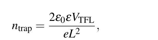

Fig.1. Characterization of SnO2 ETLs prepared by different processes. SEM image of(a)the SC-SnO2 and(b)SP-SnO2. (c)Cyclic voltammograms of the bare ITO,ITO/SC-SnO2 film,and ITO/SP-SnO2/SC-SnO2 films. The scan rate was 0.1 V/s and the electrolyte solution was 0.5 mM K4Fe(CN)6+0.5 mM K3Fe(CN)6 in 0.5 M aqueous KCl. A saturated calomel electrode (SCE) was used as the reference electrode. (d) The transmittance spectra of SC-SnO2,SP-SnO2,and SP-SnO2/SC-SnO2.

Fig.2. (a)Schematic illustration of the electron-only device with a structure of ITO/ETL/perovskite/PCBM/Ag. (b)Space-charge-limited-current(SCLC)analysis of the electron-only devices. (c)Steady-state photoluminescence spectra and(d)time-resolved photoluminescence decay curves of perovskite films deposited on the bare glass,SC-SnO2 film,and SP-SnO2/SC-SnO2 film,respectively.
whereeis the elementary charge,Lis the thickness of the perovskite film (~800 nm),ε0is the vacuum permittivity, andεis the relative permittivity.[32]The spacecharge-limited current (SCLC) results manifest that theVTFLfor SC-SnO2and SP-SnO2/SC-SnO2based devices is 0.24 V and 0.12 V, respectively. Hence the corresponding calculated trap density is 1.46×1015cm-3and 7.28×1014cm-3. The trap density of the perovskite film deposited on SP-SnO2/SC-SnO2is much lower than that on the SC-SnO2. This result implies that ETL with pinholes may lead to defective perovskite films. To evaluate the defects in the ETL, SCLC experiments adopting the device structure of ITO/ETL/Ag were also performed.The results in Fig.S1 show that theVTFLfor SC-SnO2and SP-SnO2/SC-SnO2based devices is 1.89 V and 1.43 V, respectively, which indicates that the trap density in the SP-SnO2/SC-SnO2is lower than that in the SC-SnO2.
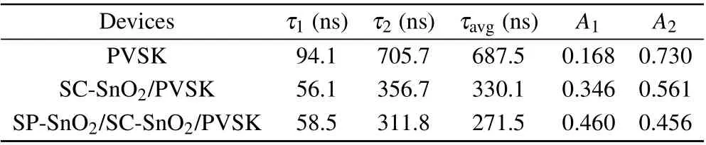
Table 1. Fitted parameters of TRPL results of wide-bandgap perovskite films without and with SP-SnO2 interlayer.
To study the role of the SP-SnO2interlayer on the charge transfer, we monitored the steady photoluminescence (PL)of the perovskite films deposited on the different substrates(Fig.2(c)). PL spectra of perovskite films deposited on ETLs exhibit lower peak intensity than that deposited on the bare glass, indicating that both ETLs enable efficient electron injection at the ETL/perovskite interface. Moreover, the perovskite film deposited on the SP-SnO2/SC-SnO2film demonstrates the best electron-extraction ability. Figure 2(d) shows the time-resolved photoluminescence(TRPL)decay curves of perovskite films deposited on different substrates. The decay curves are fitted with a bi-exponential function, and the fitting parameters are provided in Table 1. The calculated average carrier lifetime(τavg)of the perovskite films deposited on glass and SC-SnO2film is 687.5 ns and 330.1 ns,respectively.In contrast,the perovskite film deposited on the SP-SnO2/SCSnO2film shows the fastest decay with aτavgof 271.5 ns,suggesting the most efficient charge transfer. These results are consistent with the steady-state PL results.

Table 2. Photovoltaic parameters of ST-PSCs with SP-SnO2 interlayer.
We fabricated the complete ST-PSCs based on the SPSnO2/SC-SnO2ETLs. The device structure of glass/ITO/SPSnO2/SC-SnO2/perovskite/Spiro-OMeTAD/MoO3/ITO is depicted in Fig. 3(a). The SP-SnO2interlayer was inserted between the commercialized ITO and the SC-SnO2. The crosssectional SEM image in Fig. 3(b) confirms the device structure. To investigate the dependence of the device performance on the interlayer thickness,a batch of complete ST-PSCs was fabricated, and the photovoltaic metrics were measured under simulated AM 1.5G conditions. The statistics of the photovoltaic performances are shown in Figs. 3(c)–3(f), and the photovoltaic parameters are summarized in Table 2. It can be observed that theVOCincreases obviously after inserting an SP-SnO2interlayer. The averageVOCincreases from 1.162 V to 1.189 V (from the control to 18 nm SP-SnO2). This indicates that the incorporated SP-SnO2effectively suppresses the carrier recombination. The short-circuit current density(JSC)slightly decreases with the increase of the interlayer thickness, and the averageJSCdecreases from 19.17 mA·cm-2to 18.86 mA·cm-2from the control to the 18 nm SP-SnO2based device. This result can be ascribed to the parasitic light absorption of the inserted SP-SnO2. For the FF,it first increases from 69.67% to 72.25% and 73.19% from the control to the device with 6 nm and 12 nm SP-SnO2and then decreases to 71.75%for the device with 18 nm SP-SnO2. As the compact SP-SnO2blocks the pinholes of the SC-SnO2,the FF and theVOCof the devices are expected to be enhanced due to the suppression of non-radiative recombination. However, when the interlayer thickness is too large, the series resistance will increase,which sacrifices the FF.Interestingly,it can be seen that the FF of the devices with SP-SnO2interlayer with all of the investigated thicknesses is higher than that of the control,implying that non-radiative recombination is the dominant issue that limits the FF of the device based on SC-SnO2. Combining the effect of the SP-SnO2interlayer onVOC,JSC, and FF,the ST-PSCs with 12-nm SP-SnO2demonstrate the best average PCE of 16.56%. We also explored the dependency of the device performance on the thicknesses of SC-SnO2coupled with 12 nm SP-SnO2. The thickness of SC-SnO2prepared by using the SnO2precursor solution with a concentration of 5 wt.% is about 25 nm. We tuned the thicknesses of the SCSnO2layer by altering the concentration of the SnO2solution(2.5%, 5%, and 7.5%). The statistics of the photovoltaic parameters in Fig. S2 and Table S1 show that the devices with 5%SnO2achieve the best photovoltaic performance.
The hysteresis effect of these two types of devices is examined by the reverse (scanned from the open circuit to the short circuit) and forward (scanned from the short circuit to the open circuit)J–Vcurves (Fig. 4(a)). The detailed photovoltaic properties are shown in Table 3. We obtained a hysteresis index (HI) of 8.81% (PCEreverseis 17.70% and PCEforwardis 16.14%) for the SP-SnO2interlayer-based device, which is lower than that of the control (HI = 15.26%;PCEreverseis 16.91% and PCEforwardis 14.33%). The champion device demonstrates high efficiency of 17.70% with aJSCof 18.86 mA·cm-2,VOCof 1.219 V, and FF of 76.97%.The incident photon-to-electron conversion efficiency(IPCE)of these two devices is shown in Fig.4(b). The integratedJSCfor the control and the device with 12-nm SP-SnO2interlayer is 18.9 mA·cm-2and 19.0 mA·cm-2, respectively. This is well-matched with theJSCderived from theJ–Vcurves. The electrochemical impedance spectroscopy(EIS)was also conducted to further analyze the charge transport in the devices.The experiment was carried out in dark conditions under a 1.0 V voltage bias to reveal the recombination process. As shown in Fig.4(c),the device with SP-SnO2interlayer exhibit a much larger semicircle than that of the control device,indicating a much larger recombination resistance.[33]This means that the recombination process could be effectively suppressed as the SP-SnO2interlayer was implanted in the ETL.

Fig.3. (a)Schematic diagram,and(b)cross-sectional SEM of ST-PSC device based on SP-SnO2/SC-SnO2 ETLs. Statistics of photovoltaic metrics of the ST-PSCs without(control)and with different thicknesses of SP-SnO2 interlayer. (c)VOC,(d)JSC,(e)FF,and(f)PCE.
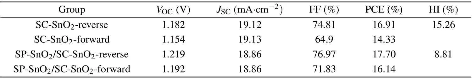
Table 3. Photovoltaic parameters of the SC-SnO2 and SP-SnO2/SC-SnO2 based ST-PSCs under the reverse and forward scan.
Stability is an important issue in PSCs. We examined the effect of the SP-SnO2on the device stability of the STPSCs. The short-term operational stability of PSCs was evaluated by monitoring the power output at the maximum power point(MPP)conditions under AM 1.5G solar simulator. MPP tracking of the device with SP-SnO2interlayer at 1.01 V shows a 5-minutes stabilized efficiency of 17.04% (Fig. 4(d)). The decline is much slower than the control. For the long-term shelf stability, we monitored the efficiency of the devices after storage for over 30 days in the drying cabinet(the relative humidity was about 10%) in the air (Fig. 4(e)). The device with the SP-SnO2interlayer displays better stability,retaining 95% of its initial PCE after 34 days. In contrast, the control device dropped to 84%of its initial PCE after the same time.These results indicate that the device stability of the ST-PSCs has been distinctly enhanced after inserting an SP-SnO2interlayer, most probably due to the suppressed recombination at the perovskite/ETL interface.
4. Conclusion
In summary, we provide a simple strategy of constructing the pinhole-free ETL for achieving efficient and stable STPSCs. This SP-SnO2/SC-SnO2ETL can integrate the advantages of SP-SnO2and SC-SnO2. The SP-SnO2interlayer can effectively increase the ETL’s compactness and the blocking ability for the photo-generated carriers, while the upper SCSnO2retains its efficient electron-extraction property. This improved ETL can significantly reduce the interfacial charge recombination, which contributes to improving theVOCand FF of the device. We obtained a high PCE of 17.70% with a stabilized efficiency of 17.04% and robust device stability for the ST-PSCs. This work provides a strategy for obtaining high-quality ETL to promote the efficiency and stability of perovskite solar cells.
Acknowledgments
This work was financially supported by the National Natural Science Foundation of China (Grant Nos. 22179042,U21A2078, and 51902110), the Natural Science Foundation of Fujian Province, China (Grant Nos. 2020J06021,2019J01057, and 2020J01064), Scientific Research Funds of Huaqiao University, and Promotion Program for Young and Middle-aged Teacher in Science and Technology Research of Huaqiao University(Grant Nos.ZQN-PY607 and ZQN-806).

- Chinese Physics B的其它文章
- A design of resonant cavity with an improved coupling-adjusting mechanism for the W-band EPR spectrometer
- Photoreflectance system based on vacuum ultraviolet laser at 177.3 nm
- Topological photonic states in gyromagnetic photonic crystals:Physics,properties,and applications
- Structure of continuous matrix product operator for transverse field Ising model: An analytic and numerical study
- Riemann–Hilbert approach and N double-pole solutions for a nonlinear Schr¨odinger-type equation
- Diffusion dynamics in branched spherical structure