传输栅掺杂对CMOS有源像素满阱容量及暗电流的影响
2022-11-26 03:43王倩徐江涛高志远陈全民
光子学报 2022年11期
王倩,徐江涛,高志远,陈全民
(天津大学微电子学院天津市成像与感知微电子技术重点实验室,天津 300072)
0 Introduction
In recent years,Pinned Photodiode(PPD)CMOS Image Sensors(CISs)are widely used in consumer electronics and other fields due to their high performance and low cost[1].CMOS active pixels play an important role in CISs.The design of the Transfer Gate(TG)affects image quality,which is related to Full Well Capacity(FWC)and dark current[2-4].TG affects the feedforward effect by channel potential.The feedforward effect directly influences FWC as the charges in PPD can flow into Floating Diffusion(FD)by thermal emission[5].In addition,due to the existence of interface states,the dark current generates at the interface of the TG channel,which flows into PPD during the integration period[6].
Several papers have analyzed the influence of TG on FWC and dark current,and have proposed different improvement techniques and designs.A negative bias operation of TG is an effective method to reduce dark current under TG[7-9].When a negative bias is added to TG,the channel is in a state of accumulation,isolating the interface state of the channel from the depletion region of PPD so that dark current is greatly reduced.Furthermore,adopting a negative bias to TG increases the channel barrier,inhibiting the feedforward effect and increasing FWC.A positive voltage adopted to TG is also beneficial to reduce dark current due to the sharing mechanism[6],but will make FWC decrease.To reduce dark current,Ref.[10]has proposed a method to change the position of the potential barrier under TG by adjusting the doping length of p-type impurities so that dark charges could flow to FD.This paper investigates the influence of two types of doped transfer gates,named N+TG and P+TG,on FWC and dark current.P-type doping is shared with p+doping used in PMOS transistors,so no additional steps need to be introduced.The channel potential is affected by the work function difference between TG and the substrate.A higher potential barrier between the TG channel and PPD can effectively suppress the feedforward effect and increase FWC.In addition,accumulated channels can reduce dark current.
1 Impact of TG doping on FWC and dark current
1.1 Work function influence on TG channel potential
To analyze the influence of TG doping on FWC and dark current,a typical 4T-PPD pixel structure is used in this paper.The device cross section is shown in Fig.1,which consists of a PPD,a“special”TG transistor whose drain is a Floating Diffusion(FD)node,and three conventional transistors named Reset Transistor(RST),Source Follower(SF),and Row Select(RS)transistor.P+TG and N+TG are adopted in this paper.The p-type heavy doping range is in the middle region of TG,0.1 μm away from the TG edge.The ntype heavy doping edge of FD is next to the p+doped boundary on the right side of TG.The upper left corner of Fig.1 shows the N+TG structure,and the two kinds of TG have the same structure except for different doping types.To ensure the smooth transfer of charges from PPD to FD,PPD implantation usually extends slightly under TG to assist charge transfer.At the same time,two p-type implantations are carried out under TG,named TG_PD and TG_FD,for threshold adjustment and anti-punch-through respectively.Before illumination,RST opens to reset PPD and FD.The photo-generated electrons are collected and stored by PPD during illumination.After an exposure period,the photoelectric charges in PPD are transferred to FD by switching on TG,where the signal in the charge domain is converted to the voltage domain.When RS is switched on,the signal is buffered to the column bus by SF.
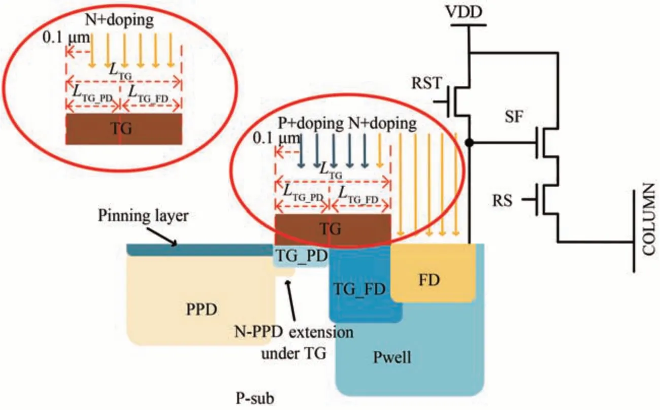
Fig.1 4T-PPD pixel structure profile of P+TG and N+TG
The impact of TG doping on FWC and dark current is achieved by channel potential,which is affected by the work function of TG and the substrate.P+TG is proposed in the paper.Fermi energy level of P+TG is near the valence band.The work function difference(Wms-p)between P+TG and the p-type substrate is calculated by
whereEgis the silicon forbidden bandgap,KTln(Na/ni)represents the difference between the central bandgap energy of the substrate and Fermi energy level,Kis the Boltzmann constant,Tis the absolute temperature,Nais the doping concentration in the channel region of the substrate,niis the intrinsic carrier concentration in silicon at room temperature(300 K).According to the physics of semiconductors[11],part of the voltage caused by the work function difference and traps falls on the oxide layer,while the other part falls on the channel interface.

whereNtrapis the density of traps,the typical value ofNtrapis 1×10¹⁰traps·cm-2,σsis the effective capture cross-section(In the simulation,σsis set to 1×1-14cm2),Cois the gate capacitance per unit area,Co=εo×εr/d,Vspis the interface potential of P+TG channel,Qspaceis the density of interface space charge.Substituting the parameters in Table 1 into Eqs.(1)and(2),the left side of the formula is negative after calculation.The work function difference has a higher effect than traps,and the channel interface is in an accumulated state.Qspaceuses the metal-insulator-semiconductor model to calculate according to the formula in the accumulative state[11].
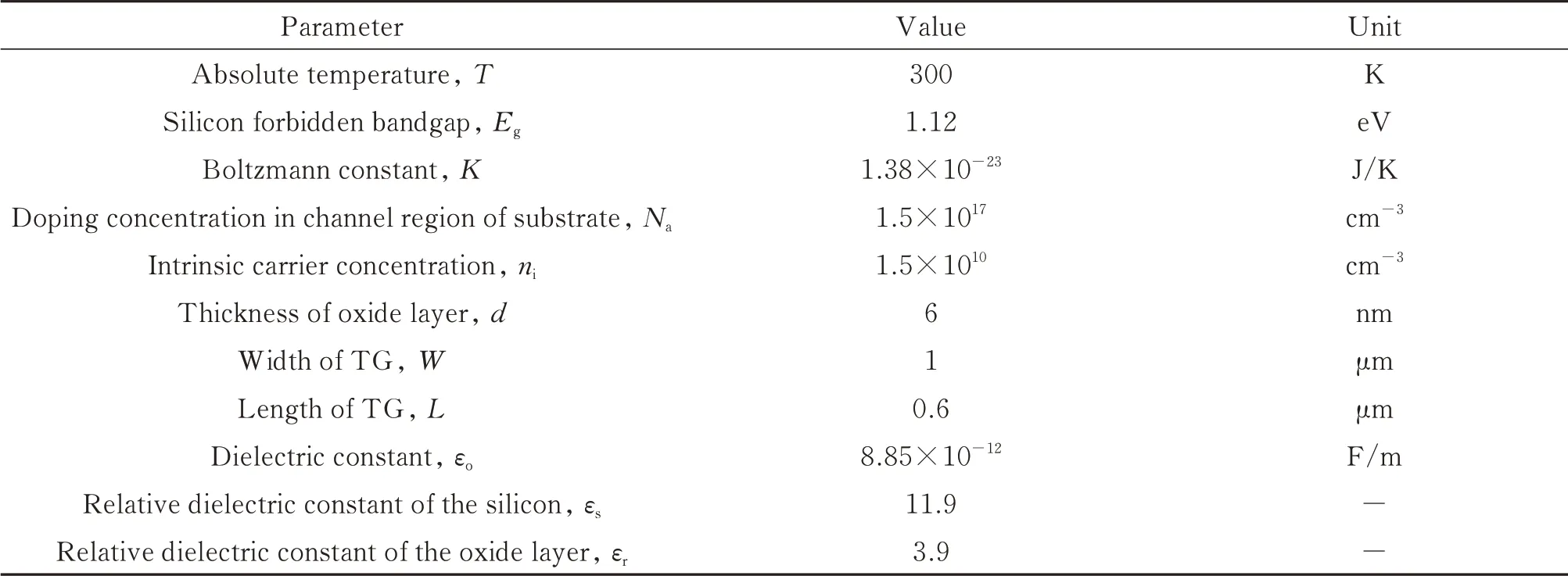
Table 1 The design parameters in this paper

whereLDis the Debye length,LD=((εoεsKT)/(q2Na))1/2,εsis the relative dielectric constant of silicon.Combined with Eqs.(1),(2)and(3),we can get thatVspis-0.03 V.Generally,traditional TG is heavily doped with n-type impurities.The Fermi energy level of N+TG is near the conduction band.The work function difference isWms-n=-Eg/2-(KT)ln(Na/ni).In the same analysis as above,the interface potential of the N+TG channel,namedVsn,is calculated by using the depletion approximation method,andVsnis 0.66 V.Therefore,the channel potential of P+TG is lower than that of N+TG.A higher barrier between the TG channel and PPD is conducive to inhibiting the feedforward effect.
1.2 TG doping influence on FWC and dark current
FWC is an important parameter of CIS.The feedforward effect is the main reason for the decrease in FWC.Fig.2 shows the potential diagram along the emission current path with TG off.The lower potential of the channel,the more difficult it is for the electrons in PPD to enter FD through thermal emission.In Ref.[12],when PPD reaches FWC,there is an equilibrium of three main currents in PPD:the light currentIph=ƞΦph,the sub-threshold currentIDS(mainly caused by the feedforward effect),and the forward currentIfwof PPD.
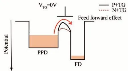
Fig.2 Potential diagram along the emission current path of P+TG and N+TG
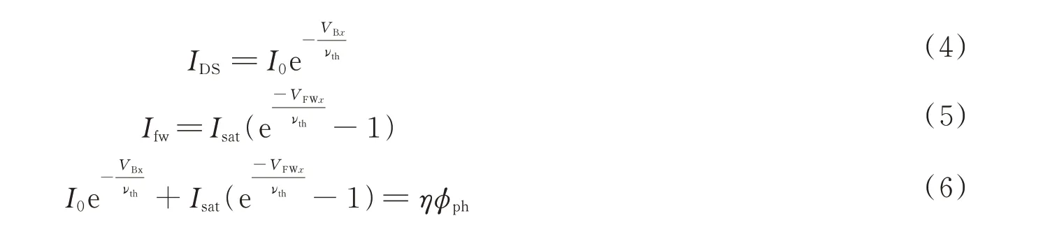
whereI0is the current coefficient,depending on the Richardson constant,the cross-sectional area of the transfer path(PPD-TG interface),and temperature.The subscriptxin the symbols mentioned below represents different doping types of TG,taking n and p respectively.VBxis the height of the potential barrier between the TG channel and PPD at the full well,which is represented asVBx=VFWx-Vsxhere,VFWxis the PPD voltage at the full well,andIsatis the reverse saturation current through PPD.According to the analysis in Section 1.1,we know thatVsnis greater thanVsp.Combined with Eqs.(4),(5)and(6),it can be concluded thatVFWpis smaller thanVFWn.In addition,VBn<VBpcan also be obtained.The higher barrier can effectively inhibit the feedforward effect.Ignoring the generation and recombination process of the PPD region,FWC can be approximately expressed as the maximum voltage swing of PPD multiplied byCPPD:

whereVpinis the maximum potential variation of hole and electron quasi-Fermi level,in general,the voltage after PD reset isVpin,QFWxis the FWC of PPD.Obviously,QFWn<QFWp,the FWC of P+TG is improved compared with that of N+TG.
In a 4T-PPD pixel,the main dark current contributor is the traps at the silicon-oxide interface under TG[6].Dark current caused by traps can be expressed as Ref.[14].

whereνthis the thermal velocity.Combined with the previous analysis,the P+TG channel is in a state of accumulation,isolating the depletion region of PPD from the interface states below TG.The dark current generated by traps is compensated,resulting in the reduction of dark current.
2 Simulation results
A 4T-PPD is simulated in Technology Computer Aided Design(TCAD).The same trap model as Ref.[6]is added to the simulation.We set the concentration of traps to 1×10¹⁰traps·cm-2and the capture crosssection to 1×10-14cm2[10,15-16].PPD of two doping types of TG integrates for 10 ms in dark conditions.In addition,the light intensity is set to 2×10⁻³W/cm2when testing the FWC of PPD.This paper compares P+TG and N+TG under the same channel and substrate doping conditions.FWC and dark current characteristics are simulated when the turn-off voltage(VTG_off)is 0 V.
To prevent punch-through,LTG_PDandLTG_FDare set to 0.3 μm by default.We set the left side coordinate of TG to 5.0 μm.Given FWC and charge transfer problem,the length of TG is set to 0.6 μm.Fig.3 shows the simulation cross-section with two doping types of TG.The white line is the depletion zone boundary.As shown in Fig.3,the N+TG channel is depleted.For a more intuitive view of the results,Fig.4 shows the onedimensional electrostatic potential distribution intercepted by two doping types of TG along theX-X′(X-X′is 0.01 μm away from the channel interface)and along theY-Y′(Y-Y′is located in the middle of TG),respectively.It is obvious thatVsnof N+TG is greater than zero.Vspobtained by the simulation is-0.032 V,which is slightly different from the previous theoretical calculation of-0.03 V,due to the simulation deviation.P+TG has a higher potential barrier which can better inhibit the feedforward effect.The potential distribution fully indicates that the channel of P+TG is in the state of hole accumulation.FWC with two types of doped TG is shown in Fig.5(a).The values are normalized using FWC of N+TG as the standard.Due to the lower channel potential of P+TG,the ability to suppress the feedforward effect is stronger,and FWC is higher.Compared with N+TG,the FWC of P+TG is increased by 26.5%.Furthermore,Fig.5(b)shows the number of dark charges integrated by PPD of two types of doped TG in 10 ms,which is normalized based on the dark charges(Ndark)of N+TG.Dark current of P+TG is 0.377 times that of N+TG.According to the above analysis,P+TG has better FWC and dark current characteristics whenVTG_offis 0 V.In practical engineering,a negative voltage is usually applied to N+TG during exposure to obtain good full well capacity and dark current characteristics.As shown in Fig.6,FWC and dark current for two types of TG at variousVTG_offare obtained.With the decrease of negative voltage,channel potential decreases,so the feedforward effect is inhibited,and the FWC of two types of TG increases.WhenVTG_offis less than-0.8 V,the FWC of N+TG is higher than that of P+TG at 0 V.As the negative voltage added to N+TG is less than-0.2 V,the depletion zone of PPD is disconnected from the depletion zone of TG channel,and the channel of N+TG accumulates gradually.Dark current of N+TG reduces withVTG_offdecreases.WhenVTG_offis greater than-0.2 V,dark current of N+TG decreases due to the sharing mechanism.For P+TG,the negative voltage has little effect on the dark current because the channel is accumulated.The introduction of negative voltage can improve the full well capacity and dark current characteristics of N+TG,increasing in power consumption.

Fig.3 Two-dimensional simulation profiles
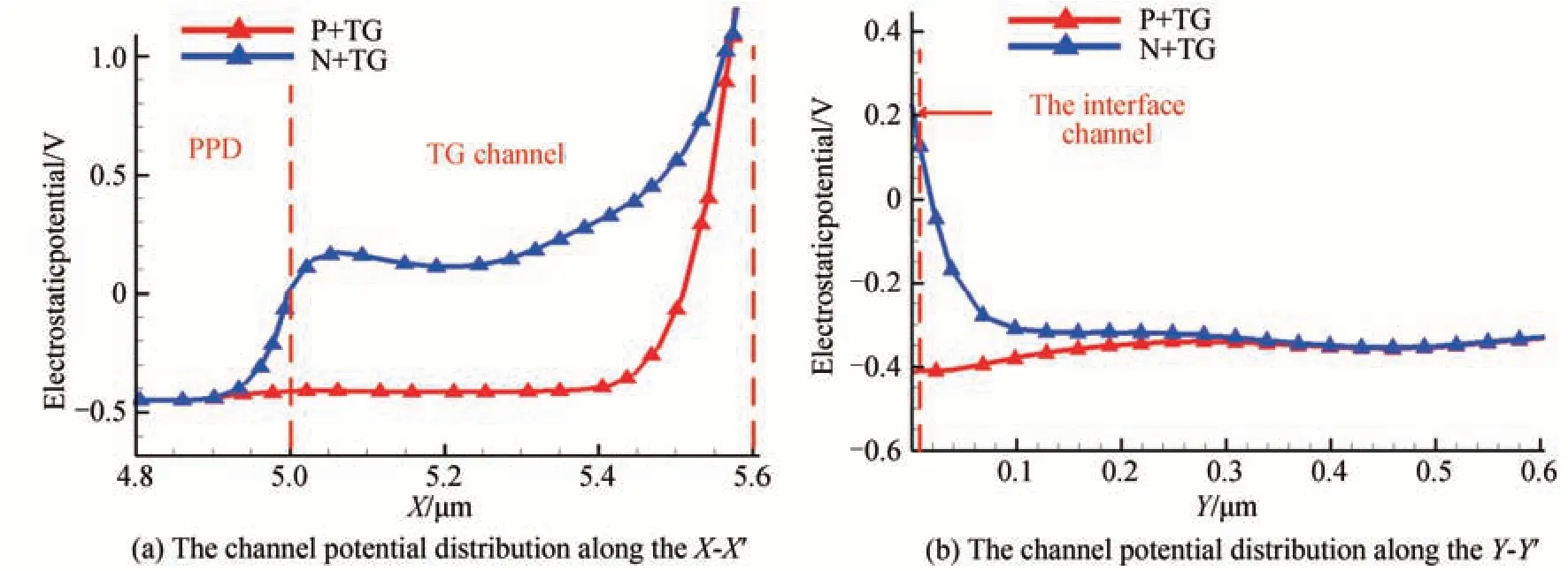
Fig.4 One-dimensional potential diagrams under TG
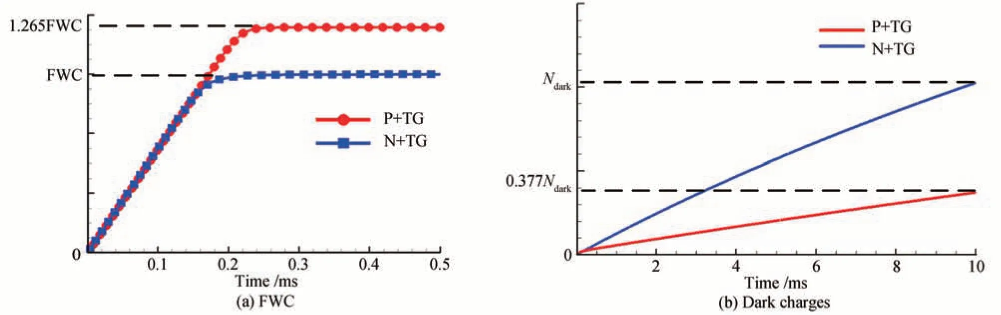
Fig.5 Simulation results of FWC and dark charges with two types of doped TG at 0 V
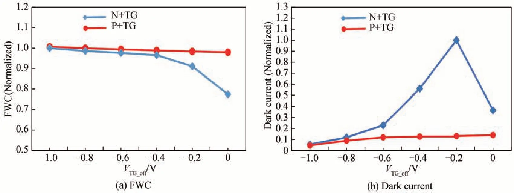
Fig.6 Simulation results of FWC and dark current with two types of doped TG at various VTG_off
The opening characteristics of TG affect image lag,which plays an important role in imaging quality and is usually determined by Charge Transfer Efficiency(CTE)[17].

whereQOUTis charges transferred from PPD to FD.The TCAD tool is used to study the CTE of P+TG and N+TG.In the simulation,the charge transfer characteristic with opening voltage(VTG_on)of TG from 0 V to 3.3 V is simulated.As shown in Fig.7,whenVTG_onincreases,CTE improves and finally tends to be stable,approaching 100%.BeforeVTG_onis 3.0 V,the transfer characteristic of N+TG is better than that of P+TG because of the higher channel potential.The charge transfer characteristic is controlled byVTG_on.Specially,the CTE of N+TG is greater than 99.999% at 2.3 V,while P+TG requires 3.0 V.AsVTG_on(>3.0 V)continues to rise,the CTE of N+TG and P+TG shows no difference,suggesting that charges can be completely transferred from PPD to FD.Universally,the opening voltage of TG is 3.3 V,Fig.8 shows the potential profile with TG on.The channel potential of N+TG is higher than that of P+TG.Moreover,the potential gradually increases from the left side to the right side,and charges can be transferred smoothly along the transfer path.This is the ideal situation for simulation.In actual devices,CTE may be lower than the simulation results because of process deviation and annealing process.When the FWC of PPD is high,CTE will be negatively affected,resulting in image lag.At this point,the positive charge pump needs to be introduced to ensure transfer characteristics.Under the simulation conditions in this paper,two doping types of TG have good transfer characteristics at 3.3 V.
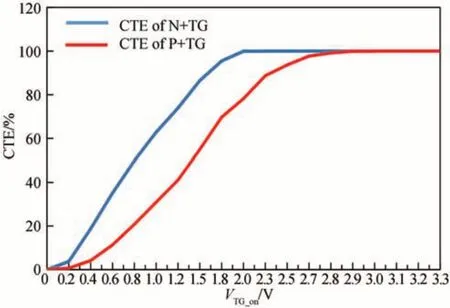
Fig.7 Simulation results of CTE with P+TG and N+TG
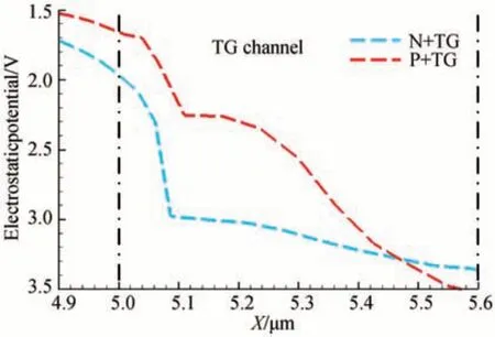
Fig.8 One-dimensional potential diagram under TG channels with TG on
3 Conclusion
The influence of TG doping on FWC and dark current is analyzed in this paper.The channel potential of P+TG is lower than that of N+TG because of the work function difference between TG and substrate.The higher barrier inhibits the feedforward effect and increases FWC.On the other hand,the channel of P+TG is in a state of accumulation.The interface state under P+TG is isolated from PPD and dark current decreases.Device level simulation using TCAD is performed,whenVTG_offis 0V,the full well capacity of the photodiode based on P+TG is 26.5% higher than that of N+TG,and the dark current is 0.377 times that of N+TG.N+TG can optimize FWC and dark current performance by adding negative voltage.In addition,the CTE of N+TG is greater than 99.999% at 2.3 V,while P+TG requires 3.0 V.The voltage applied to P+TG is higher than that to N+TG for complete charge transfer.
猜你喜欢
趣味(数学)(2022年5期)2022-07-29
趣味(数学)(2022年5期)2022-07-29
趣味(数学)(2022年5期)2022-07-29
航天返回与遥感(2020年2期)2020-05-21
中学生英语·中考指导版(2019年12期)2019-01-03
汽车实用技术(2018年22期)2018-12-05
电子制作(2018年17期)2018-09-28
客车技术与研究(2016年3期)2016-09-07
消费电子(2016年9期)2016-05-14
红外技术(2016年3期)2016-03-28