
Unconventional room-temperature negative magnetoresistance effect in Au/n-Ge:Sb/Au devices
2024-03-25 09:33XiongHe何雄FanLiYang杨凡黎HaoYuNiu牛浩峪LiFengWang王立峰LiZhiYi易立志YunLiXu许云丽MinLiu刘敏LiQingPan潘礼庆andZhengCaiXia夏正才
Chinese Physics B 2024年3期
Xiong He(何雄), Fan-Li Yang(杨凡黎), Hao-Yu Niu(牛浩峪), Li-Feng Wang(王立峰), Li-Zhi Yi(易立志),Yun-Li Xu(许云丽), Min Liu(刘敏), Li-Qing Pan(潘礼庆),†, and Zheng-Cai Xia(夏正才),‡
1Hubei Engineering Research Center of Weak Magnetic-field Detection,College of Science,China Three Gorges University,Yichang 443002,China
2Wuhan National High Magnetic Field Center,Huazhong University of Science and Technology,Wuhan 430074,China
Keywords: magnetoresistance,germanium-based devices,pulsed high magnetic fields
1.Introduction
Magnetoresistance (MR) effect has attracted extensive attention due to its extensively applications in the fields of information storage and magnetic sensing.[1-4]Meanwhile,the devices based on the MR effect in magnetic materials have been widely applied and have yielded substantial economic benefits.[5]For non-magnetic semiconductor materials and their devices, huge positive MR effect and abundant physical phenomena have been observed under low static magnetic fields by constructing devices with different geometric configurations,[6-9]designing different heterojunction structures,[10-15]choosing substrate materials with different doping concentrations,[16]introducing a photoinduced environment,[17]regulating external electric fields,[18-21]and so on.Therefore,non-magnetic semiconductors and their devices are very important application prospects.
Under a pulsed high magnetic field,the charged particles or magnetic moments of the material may be easily affected,resulting in a change in the state of motion of the particles or the magnetic properties of the material.Consequently, the electrical and magnetic properties of materials or devices may exhibit new phenomena different from those under low static magnetic fields.For example, Heet al.[22]observed an obvious MR retraction behavior in Ag/p-Ge:Ga/Ag device under 45 T pulsed high magnetic field.Wanget al.[23]discovered a new type of log-periodic oscillations behavior in ZrTe5under 60 T pulsed high magnetic field.Zhuet al.[24]found a significant drop in the resistance of the half-metal Bi under high magnetic fields (higher than 35 T).The interaction between spin and lattice degrees of freedom in ErFeO3,[25]LuFe2O4,[26]MnV2O4[27]and other multiferroic materials can be regulated effectively by pulsed high magnetic fields.Thus, for nonmagnetic semiconductor materials and their devices, a more adequate study of their transport properties under higher magnetic fields is required.
In this paper, the room-temperature MR properties of Au/n-Ge:Sb/Au device with identical side metal electrodes under a 50 T magnet are investigated.We observe an obvious unconventional negative MR effect in a specific pulsed high magnetic field direction,while not find this effect under static low magnetic fields.The relevant microphysical mechanisms have been carefully discussed and confirmed.
2.Experimental details
In this study,the Au/n-Ge:Sb/Au device was prepared by high vacuum magnetron sputtering Au electrode on the lightly antimony (Sb)-doped Ge (n-Ge:Sb)〈100〉-oriented crystal wafer with room temperature resistivity of 1-10 Ω·cm.The doing concentration of Sb and Hall mobility at 300 K are about 1.68×1015cm-3and 1.35×103cm2·V-1·C-1,respectively,which are measured by using the van der Pauw method.Considering the possible eddy current thermal effect under pulsed high magnetic field, we cleave the wafer into strips and reduce the lead circuit as much as possible.The static low magnetic field is provided by a physical property measurement system, and the electrical transport properties measurement of the pulsed high magnetic field is provided by the Wuhan National High Magnetic Field centre.The electrical transport properties of the device were measured by a four-probe method, and the Hall voltage (VH) signal of the device under different conditions was obtained by the Hall bar method.The obtainedVHvalues under positive and negative magnetic fields were anti-symmetrically treated to depress the possible influence of resistance signals.In order to study the possible modulation of the strong magnetic field on the surface charge transport properties, the voltage detection electrodes are located on the identical longitudinal side and perpendicular to the electric field direction.The MR under a constant current condition is expressed as MR=(V(B)-V(0))×100%/V(0),where theV(B)andV(0)are the measured voltages under an applied magnetic field and zero magnetic field,respectively.
3.Results and discussion
The x-ray diffraction (XRD) results of the wafer and its corresponding powder are presented in Fig.1(a).We can find that the wafer is(400)-oriented,and all of the diffraction peaks of the powder are well indexed to the Ge (PDF #04-0545),indicating the used wafer is indeed lightly doped Ge.From Fig.1(b),it can be seen that the Au electrode is basically uniform and the thickness is about 82.5 nm.
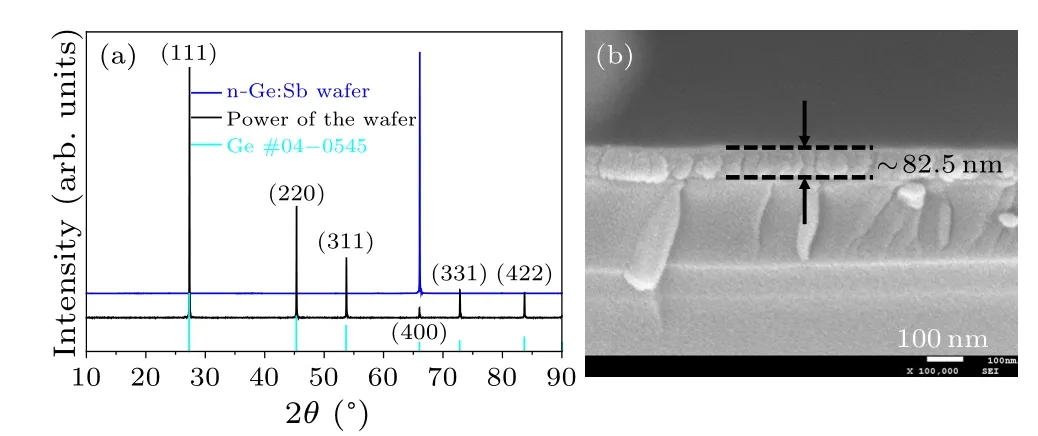
Fig.1.(a)The XRD results of the n-Ge:Sb wafer and its corresponding powder.(b)The cross-sectional morphology between the electrode Au and the semiconductor wafer.
Figures 2(a)and 2(b)present the voltage(V)versus current (I) curves of the Au/n-Ge:Sb/Au device at 300 K and zero magnetic field, where the insets are the measurement schematic diagram and the calculated resistance (R) versusIcurve, respectively.In a small current range(0 ≤I≤5 mA),theV-Icurve is a straight line across the origin,indicating that the contact between the Au electrode and n-Ge:Sb in the device can be regarded as an ohmic one.As the applied current increases, the measured voltage gradually begins to increase nonlinearly, and theRof the device also increases.Until the applied current increases to about 40 mA,theRvalue reaches the maximum.With further increase of the current,theRvalue begins to decrease.Based on these transport properties,we divide the applied current range into ohmic(0 ≤I≤5 mA)and two non-ohmic transport regions(i.e.,5 mA<I≤40 mA(N-I region)and 40 mA<I≤100 mA(N-II region)),respectively.According to the previous reports,[20,22]in the N-I region,theRof the device may be mainly affected by the space charge effect.When the applied current reaches about 40 mA,a strong local non-uniform electric field may be formed in the device,causing local impact ionization,and then an equivalent minority carrier injection effect is induced.[20,28]Thus, in the N-II region, theRof the device decreases with the increasing applied current.
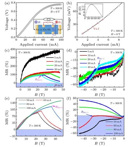
Fig.2.(a) The V-I curve of the Au/n-Ge:Sb/Au device (numbered as Q9#,the geometry size is about 1.30 mm×0.70 mm×0.30 mm)under zero magnetic field and 300 K,where the inset is the measurement diagram.(b)The locally amplified V-I curves in a small applied current range, where the inset is the calculated R-I curve.(c)-(f) The MR-B curves of the device in different magnetic field directions and different constant currents at 300 K.
In the above three transport regions, the MR properties of the device at 300 K under 50 T pulsed high magnetic field are shown in Figs.2(c)-2(f).In the ohmic region (I=5 mA as an example), the MR value of the device is positive in the pulsed positive magnetic field (B+) direction, and increases with the increment of the magnetic field strength, without showing a saturation trend.The maximum MR value within the applied magnetic field range is about 372%.This conventional unsaturated positive MR behavior is similar to that reported previously.[29]Interestingly, under the condition of pulsed negative magnetic field (B-) direction, the device exhibits an unconventional negative MR effect.The negative MR value increases sharply first and then increases slowly with the increment of the magnetic field strength, and the maximum negative MR value reaches approximately-50%.
Similarity,in the N-I region(I=10 mA,20 mA,30 mA and 40 mA as examples), the positive and negative MR behaviors can also be observed in the pulsedB+andB-directions, respectively.In addition, in the pulsedB+direction, an obvious positive MR retraction behavior (the magnetic field strength corresponding to the retraction is recorded asBth(+)) is presented.This behavior is similar to that reported in the previous work.[22]At 40 mA, the sign of the MR value changes from positive to negative slightly when the magnetic field strength reaches about 45.3 T [see Fig.2(c)].In the pulsedB-direction, the unconventional negative MR values increase with the increment of magnetic field strength.Moreover,a transition behavior of the rate of the negative MR values can be observed.We labeled this transition magnetic field strength asBth(-).TheBth(-)values decrease with the increment of the applied constant current[see Fig.2(d)].
In the N-II region, whenI=50 mA or 60 mA, the transition behavior of the rate of the unconventional negative MR values in the pulsedB-direction and the change behavior of the sign of the MR value under a stronger magnetic field in pulsedB+direction can also be observed [see Figs.2(e) and 2(f)].TheBth(+/-)values increase with the increment of the applied current.Under larger applied current conditions(such as 80 mA and 100 mA),the unconventional negative MR effect is hardly observed in both of the pulsedB+andB-directions.To our knowledge,the above room-temperature large negative MR effect in non-magnetic semiconductor materials and their devices has not been reported in the literature.[15,19,20,22,28]
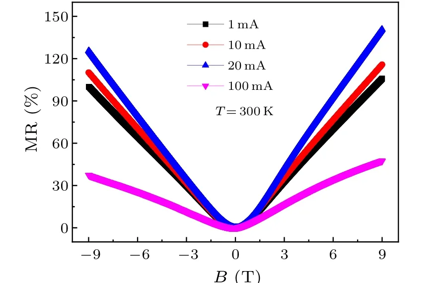
Fig.3.The MR-B curves of the Au/n-Ge:Sb/Au device (numbered as 36#, the geometry size about 1.90 mm×0.90 mm×0.30 mm,which is closer to the geometry size of device Q9#) under different applied constant currents.The sweep rate of the static magnetic field is 50 Oe/s,which is much lower than that of the pulsed high magnetic field(dB/dt >103 T/s).
We further investigate the MR properties of the device at different static low magnetic fields (with very low sweep rate of 50 Oe/s), the results are displayed in Fig.3.Conventionally, we can find that the values of MR in staticB-direction are slightly smaller than that of the MR in staticB+direction under the same magnetic field strength, presenting a weak asymmetric MR behavior.Furthermore, in the three transport regions,the MR values are positive and increase with the increment of magnetic field strength.This conventional unsaturated MR feature is analogous to the previous works on the MR effect of non-magnetic semiconductor materials and their devices.[20,22,28,30-32]However,we cannot observe negative MR effect in the static low magnetic field environment.

Fig.4.(a) The RH-I curves of the Au/n-Ge:Sb/Au device 36# under different static magnetic fields.(b) The nqRH-p/n curve of an n-type semiconductor based on the bipolar transport model.
To clarify the evolution mechanism of the MR properties of the device under pulsed high magnetic field, we investigate the Hall effect of the device.According to the formulaRH=(d/I)×(VH/B), the Hall coefficient (RH) values are obtained.TheRH-Icurves under static magnetic fields are shown in Fig.4(a).The values of theRHare negative in the applied current range, indicating that the transport properties of the device are indeed dominated by electrons under zero magnetic field and low magnetic field conditions.In the ohmic region,the absolute value of theRHis relatively large and varies slightly with the applied current, indicating that the injection of the minority carrier (i.e., hole) is basically ignored.With the increment of the applied current,the absolute value of theRHdecreases sharply in the N-I region,and then begins to decrease slowly in the N-II region and tends to zero eventually,suggesting that the holes are indeed effectively injected into the device in these two non-ohmic transport regions.According to the bipolar transport model,theRHcan be expressed by the formulaRH=[pµ2p-nµ2n]/[q(pµp+nµn)2], where thenandpare the concentrations of electrons and holes,µnandµpare the mobility of electrons and the mobility of holes,respectively.[33,34]Theqis the amount of charge.At 300 K,theµn/µpvalue of the lightly Sb-doped n-Ge is about 2.[35]Thus the simulated normalizedRH(=nqRH)can be expressed asnqRH= (p/n-4)/(p/n+2)2.Similar to the preceding work,[33]we use the normalizedRHto analyze the change ofRHwith the ratio ofp/nqualitatively.According to the normalizedRH-p/ncurve [see Fig.4(b)], the normalizedRHvalues are negative, which is in agreement with the n-type conductive of the Ge wafer.As thep/nvalue increases,the absolute value of the normalizedRHdecreases sharply first and then decreases slowly.Whenp/n=4, the normalizedRHvalue is zero.If thep/nvalue continues to increase, theRHvalue will increase to a small positive value, which means that the conductive type in the device will change from n-type to ptype.Comparing the results presented in Figs.4(a) and 4(b),it can be expected that this change will require a large applied current in an actual n-type device.The continuous increment of the applied current will be accompanied by non-negligible Joule heating and other factors, so the actual scenario of this change will be difficult to be observed.In the case ofp/n <4,the variation of normalizedRHwithp/nis similar to that ofRHwith the applied currentI,suggesting that in the two nonohmic transport regions,the holes are effectively injected into the device from the anode, and the electrons are transported from the cathode.The larger the applied current is,the higher the effective hole concentration will be injected.In addition,in the case of the applied large current,the hole concentration is comparable to the electron concentration in the device.
TheVH-Bcurves under the 50 T pulsed high magnetic field are shown in Figs.5(a) and 5(b).In the ohmic region(I=5 mA as an example), the slope of theVH-Bcurve is indeed negative.In the two non-ohmic transport regions (except for the smaller current of 10 mA and the larger current of 100 mA), the slopes of theVH-Bcurves show significant change from negative to positive under different constant current conditions, indicating that the holes gradually begin to dominate the transport properties of the device with the increasing pulsed magnetic field strength.The corresponding transition magnetic fields in the case of pulsedB+andB-directions are labeled asBth(+)′andBth(-)′,respectively.Comparing theVH-Band the MR-Bcurves, we can find that the values of theBth(+)′andBth(-)′are nearly equal to that of theBth(+)andBth(-),respectively,indicating that the positive MR retraction and the rate of the unconventional negative MR values transition behaviors are related to the change of thep/nvalues under the modulation of the stronger Lorentz force provided by the pulsed high magnetic field.[22]
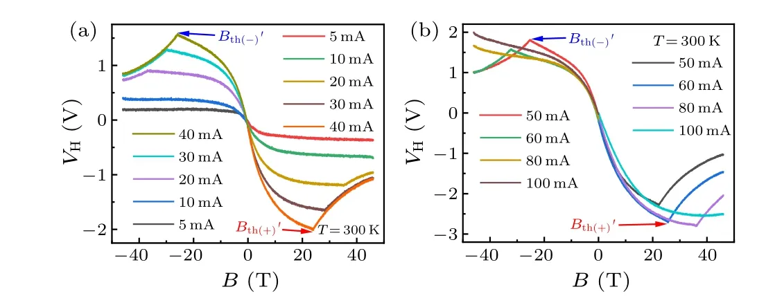
Fig.5.[(a),(b)]VH-B curves of the Au/n-Ge:Sb/Au device Q9#in different conductive regions.
For negative MR effect,due to the differences in materials,structure of devices,external environment and many other factors, a number of mechanisms have been proposed.However, the observed unconventional negative MR effect in this paper under pulsed high magnetic field conditions cannot be explained by these mechanisms.The main considerations are as follows:
The first one is the spin-dependent scattering mechanism of carriers.[36]In magnetic materials or devices, due to the spin-dependent scattering of carriers, the material exhibits a negative MR effect after applying a magnetic field.The nonmagnetic Ge-based device system in our study does not contain any magnetic materials, so this mechanism may not be suitable for the unconventional negative MR effect observed in this paper.
The second possible mechanism is the non-uniform distribution of carriers.[30,37]Under an extremely low magnetic field,the carriers in the non-magnetic semiconductor will undergo a trapezoidal re-distribution due to the Lorentz force.When the distance between the detection electrodes is small,the detected voltage will decrease with the increment of magnetic field strength(in low magnetic field range),presenting a negative MR.As the magnetic field strength continues to increase, the scattering effect of carriers is enhanced, and the positive MR effect will be gradually enhanced,resulting in the gradual transformation of the negative MR into positive MR.Obviously,this is distinct from the unconventional MR effect we have found.
The third possible mechanism of the negative MR is the localization effect.[38,39]This effect is a quantum effect,which is only observed at extremely low temperature and low magnetic field conditions.Obviously, the unconventional negative MR effect is presented at room temperature and under extremely high magnetic field in our work, which cannot be interpreted by this mechanism.
The fourth related physical mechanism is the differentresponse model of electrons and holes to the magnetic field.[40,41]Under this bipolar transport mechanism, the MR changes from positive to negative with increasing applied constant voltage.It is believed that this is related to the different magnetic field responses of hole mobility and electron mobility.However,under the condition of a constant applied electric field,no analogous phenomenon of the MR evolution behavior is observed in our work.
Finally, the possible physical mechanisms include the quantum limit effect[42]and the longitudinal negative MR related mechanism,[43-45]both of which are based on the magnetic field parallel to the direction of the electric field.Nevertheless, the applied pulsed high magnetic field is perpendicular to the direction of the applied current,so these mechanisms may not be suitable to explain the unconventional negative MR effect shown in Figs.2(d)and 2(f).
For the unconventional negative MR effect observed in this work, the Hall effect may be an influencing factor, but a relatively complex MR effect is exhibited under the pulsed high magnetic field [see Figs.2(c)-2(f)].To construct a specific microscopic physical image from the perspective of charge more clearly,we have not directly excluded the possible Hall signal by symmetrically calculating the voltage signals measured under positive and negative magnetic fields.The surface and bulk charge transport physical images of the device under different pulsed high magnetic field conditions are illustrated in Fig.6.When the magnetic field is not applied,the charge in the device can be regarded as distribution uniformly [see Fig.6(a)].In this case, the equivalent circuit at both ends of the detection electrodes is a parallel structure of the device surface resistance (Rsurface) and bulk resistance (Rbulk) [see Fig.6(b)].Thus, the resistance of the device(Rdevice)conforms to the formula 1/Rdevice=1/Rsurface+1/Rbulk.When the pulsedB-is applied, the electrons and holes in the bulk are gathered toward the surface A with the detection electrodes due to the strong Lorentz force and participate in the surface transport[see Fig.6(c)].Under the condition of a small applied current, the injected hole concentration is relatively low, and the charge gathered to the surface A will not be completely recombined,but will form a significant charge accumulation effect on the surface A.TheRsurfacevalue decreases with the increment of the pulsed magnetic field strength, forming an obvious negative feedback mechanism on the total MR effect of the device.Then, even if the bulk MR is positive,it is also possible to observe that the device exhibits the unconventional negative MR behavior in the pulsedB-direction [see Figs.2(d) and 2(f)].However, in the static low magnetic field environment, the electrons and holes will have enough time to recombine, resulting in the much weaker charge accumulation effect on the surface A.Thus, the unconventional negative MR behavior in the staticB-direction is hardly exhibited (see Fig.3).With increasing the pulsed magnetic field strength, the bulk positive MR also begins to decrease due to the further modulation on thep/nvalue.[22]Moreover, the total MR of the device will be more easily affected by the surface charge transport behavior.Thus,the unconventional negative MR effect will be further enhanced with the increment of the pulsed magnetic field strength [as shown in Figs.2(d) and 2(f)].At larger applied current (such as 80 mA and 100 mA), the injected hole concentration is no longer significantly lower than the electron concentration, resulting in a significant recombination effect of electrons and holes in the bulk and the surface A.That is,the negative feedback mechanism of charge accumulation effect on the total MR of the device will be obviously weakened,leading to the total MR effect of the device being positive even in the pulsedB-direction[see Figs.2(d)and 2(f)].This negative feedback mechanism is also backed by the phenomenon that the value of the total MR in the pulsedB-direction is relatively smaller than that of in the pulsedB+direction under the same magnetic field strength.
When the pulsedB+is applied, the positive MR retraction behavior observed is derived from the modulation of the pulsed magnetic field on thep/nin the bulk.[22]When the applied current is close to 40 mA, it can be seen from the inset of Fig.2(b) that a strong local impact ionization occurs in the device, the energy of electrons and holes are high, and the electron concentration and hole concentration in the bulk are relatively high before the pulsed magnetic field is applied.Then,in the case of the pulsedB+,the charges(electrons and holes) in the bulk adjacent to the surface A may be scattered to this surface, thereby forming the negative feedback mechanism of the total MR of the device.The stronger the pulsed magnetic field is,the higher the charge concentration captured on the surface A is,and then the more favorable it is to observe the sign change behavior of the MR value at stronger magnetic field[as shown in the MR-Bcurves corresponding to 40 mA and 50 mA in Figs.2(c)and 2(e)].In the pulsedB+direction,owing to the electrons and holes in the bulk are easily gathered away from the detection electrodes surface(i.e.,surface C),the charge accumulated on the surface C is difficult to be detected by the electrodes[see Fig.6(d)],so that the total MR detected after the application of the pulsedB+is mainly derived from the bulk MR.According to the previous reports,[3,9]in nonmagnetic semiconductor-based devices,the movement of carriers in the bulk undergoes inhomogeneity due to the Lorentz force,which is easily to exhibit a positive MR effect.That is,it is difficult to observe the unconventional negative MR effect in the pulsedB+direction[see Figs.2(c)and 2(e)].
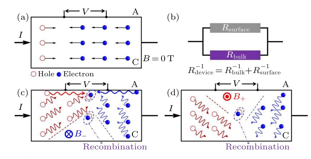
Fig.6.(a)The schematic diagram of the charge transport in the device without applied magnetic field.(b)The schematic diagram of the equivalent parallel circuit structure constituted by surface charge and bulk charge transport.[(c), (d)]The schematic diagrams of the bulk charge deflecting towards the electrode detection surface (labeled as surface A) and deviating from the electrode detection surface (labeled as surface C) under negative and positive pulsed magnetic field conditions,respectively.The charge accumulation effect formed on the surface A can be detected by the electrodes.
To further shed light on the above physical model we proposed, we investigate the MR effect of the device Q9# at different temperatures and different dB/dtof the pulsed high magnetic field, the results are presented in Fig.7.As shown in Fig.7(a), in the pulsedB+direction, the values of the positive MR increase with the decreasing temperature whenB <Bth(+)(77 K), which is similar to the previous report.[20]We are aware that the carrier mobility increases with the decrement of temperature,and the Lorentz force will also increase,so that the modulation effect of thep/nvalues will be stronger.Therefore, the positive MR retraction behavior is easier to be observed at low temperatures.Similarly,in the pulsedB-direction,the value ofBth(-)also decreases with the decrement of temperature.Moreover, as the temperature decreases, due to the enhanced Lorentz force of electrons and holes,the gathering of electrons and holes on the surface A will be more obvious,resulting in the negative feedback mechanism for the total MR of the device will also be enhanced.Consequently,the negative MR value increases with the decreasing temperature.To study the influence of the dB/dtof the pulsed high magnetic field on the negative MR effect,based on the two pulse power supply modules(abbreviated as two modules)used in the experiment in this work, we selected another six modules with a relatively smaller dB/dtvalues of the pulsed high magnetic field.The smaller the dB/dtis, the smaller the Lorentz force will be, and the weaker the gathering of electrons and holes on the surface A will be.Similarlarly, the negative feedback mechanism will be weakened under the six-module condition.In fact, the negative MR in a smaller dB/dtis indeed smaller[see Fig.7(b)].Based on the above discussion,we can be basically convinced that unconventional negative MR effect is mainly related to the surface charge accumulation effect under the pulsed high magnetic field.

Fig.7.The MR properties of the device Q9# under the pulsed high magnetic field(a)at different temperatures and(b)in the pulsed B- direction under different pulse power supply modules with different dB/dt values.
Furthermore,we choose another device with a wider geometry size (device Q10#, the width of the device is about 1.20 mm, which is approximately twice the width of the device Q9#), and compare the evolution of its MR in different conductive regions.The main results are shown in Fig.8.In contrast to the device Q9#,in the pulsedB+direction,the device Q10#exhibits similar MR properties,including the unsaturated positive MR effect,positive MR retraction,and the sign change of the MR value at a stronger magnetic field strength.Moreover,the threshold magnetic field of theVH-Bslope transition at different constant currents is also approximately equal to the threshold magnetic field corresponding to the MR retraction behavior.
However,there are some clear differences in the direction of the pulsedB-direction.Firstly,it is difficult to observe the unconventional negative MR behavior in the device Q10# in the ohmic transport region (takingI=5 mA as an example),although the MR values corresponding to the pulsedB-direction are much smaller than that in theB+direction at the same magnetic field strength.In addition, in the non-ohmic transport regions(I=10 mA,30 mA and 50 mA as examples),the MR values in the pulsedB-direction are incompletely negative.With the increase of magnetic field strength, the MR values are positive first and then change to negative after the retraction behavior [see the MR-Bcurves corresponding to 10 mA and 30 mA in Fig.8(a)].The values of the threshold magnetic fieldBth(+/-)corresponding to the MR retraction are much smaller than those corresponding to the device Q9#under the same applied current condition.This indicates that the pulsed high magnetic field may have a geometry size correlation with the modulation ability of thep/nvalues in the device,which is worthy of subsequent systematic research.

Fig.8.(a) MR-B curves and (b) VH-B curves of the wider Au/n-Ge:Sb/Au device (numbered as Q10#, the geometry size is about 2.00×1.20×0.25 mm3)in different conductive regions.
According to the physical model illustrated in Fig.6, if the width of the device is extended, the distance required for the electrons and holes to deflect to the surface A will also be increased, resulting in the negative feedback mechanism being weakened.In addition, the movement of the space of charge in the bulk increases with the increment of the width of the device, which is beneficial to enhance the inhomogeneity movement of the carriers in the bulk under an applied pulsed magnetic field, resulting in the enhancement of the positive MR effect in the bulk material.[9]Therefore, it is difficult to observe the negative MR effect in the ohmic transport region of the wider device Q10#[see Fig.8(a),I=5 mA as an example].In the non-ohmic transport regions,due to the modulation ofp/nin the bulk material by the pulsed high magnetic field,the bulk MR effect of the device exhibits a retraction behavior after reaching the threshold magnetic fieldBth(-),and then the bulk MR values decrease with the increasing magnetic field strength.At the same time, the surface charge accumulation effect is enhanced with the increasing magnetic field strength.Therefore, the unconventional negative MR effect can be reproduced in the wider device Q10#by modulating the surface charge transport under stronger pulsed magnetic field conditions.
Although large positive MR at static low magnetic fields has been declared in some non-magnetic semiconductor materials and their devices, few of them present ultra-high magnetic field properties at room temperature, especially this room-temperature negative MR effect.[6,10,15,20,22,28,46]This limits their applications in pulsed high magnetic field environment.In our Au/n-Ge/Au device, the unconventional roomtemperature negative MR effect under pulsed high magnetic field is exhibited,showing a conspicuous asymmetric MR effect.In addition, germanium is a conventional semiconductor material,which has been extensively used in high technology applications.[47]Therefore,this unique MR property will be applicable to fabricate Ge-based magnetic sensing or magnetic logic[48,49]operating in ultra-high-magnetic-field environments.
4.Conclusion
In summary, we have investigated the room-temperature MR effect of the Au/n-Ge:Sb/Au designed device (the metal electrodes of voltage detection are located on the identical side of the device) under 50 T pulsed high magnetic field.It is found that the MR of the device exhibits an unconventional negative MR effect in a specific pulsed high magnetic field direction.In addition, this negative MR effect is difficult to be observed under static low magnetic field.Analysis illustrates that this negative MR effect is mainly related to the modulation of the surface charge accumulation effect of the device by the pulsed high magnetic field.
Acknowledgments
Project supported by the Special Funding for Talents of Three Gorges University (Grant No.8230202),the National Natural Science Foundation of China (Grant No.12274258), and National Key R&D Program of China(Grant No.2016YFA0401003).
猜你喜欢
Chinese Physics B(2023年12期)2023-12-15
华人时刊(2021年15期)2021-11-27
当代人(2021年9期)2021-09-23
少先队活动(2021年5期)2021-07-22
抗癌之窗(2021年3期)2021-02-12
歌海(2020年5期)2020-11-16
书香两岸(2020年3期)2020-06-29
中国自行车(2017年11期)2017-04-04
诗选刊(2015年4期)2015-10-26

- Chinese Physics B的其它文章
- Does the Hartman effect exist in triangular barriers
- Quantum geometric tensor and the topological characterization of the extended Su–Schrieffer–Heeger model
- A lightweight symmetric image encryption cryptosystem in wavelet domain based on an improved sine map
- Effects of drive imbalance on the particle emission from a Bose–Einstein condensate in a one-dimensional lattice
- A new quantum key distribution resource allocation and routing optimization scheme
- Coexistence behavior of asymmetric attractors in hyperbolic-type memristive Hopfield neural network and its application in image encryption