
Steady-state and transient electronic transport properties of β-(AlxGa1-x)2O3/Ga2O3 heterostructures:An ensemble Monte Carlo simulation
2022-11-21 09:30YanLiu刘妍PingWang王平TingYang杨婷QianWu吴茜YintangYang杨银堂andZhiyongZhang张志勇
Chinese Physics B 2022年11期
Yan Liu(刘妍) Ping Wang(王平) Ting Yang(杨婷) Qian Wu(吴茜)Yintang Yang(杨银堂) and Zhiyong Zhang(张志勇)
1State Key Laboratory of Integrated Service Networks,School of Telecommunications Engineering,Xidian University,Xi’an 710071,China
2Key Laboratory of the Ministry of Education for Wide Band-Gap Semiconductor Materials and Devices,School of Microelectronics,Xidian University,Xi’an 710071,China
3School of Information Science and Technology,Northwest University,Xi’an 710127,China
The steady-state and transient electron transport properties of β-(AlxGa1-x)2O3/Ga2O3 heterostructures were investigated by Monte Carlo simulation with the classic three-valley model. In particular, the electronic band structures were acquired by first-principles calculations,which could provide precise parameters for calculating the transport properties of the two-dimensional electron gas (2DEG), and the quantization effect was considered in the Γ valley with the five lowest subbands. Wave functions and energy eigenvalues were obtained by iteration of the Schr¨odinger–Poisson equations to calculate the 2DEG scattering rates with five main scattering mechanisms considered. The simulated low-field electron mobilities agree well with the experimental results,thus confirming the effectiveness of our models. The results show that the room temperature electron mobility of the β-(Al0.188Ga0.812)2O3/Ga2O3 heterostructure at 10 kV·cm-1 is approximately 153.669 cm2·V-1·s-1, and polar optical phonon scattering would have a significant impact on the mobility properties at this time. The region of negative differential mobility, overshoot of the transient electron velocity and negative diffusion coefficients are also observed when the electric field increases to the corresponding threshold value or even exceeds it.This work offers significant parameters for the β-(AlxGa1-x)2O3/Ga2O3 heterostructure that may benefit the design of high-performance β-(AlxGa1-x)2O3/Ga2O3 heterostructure-based devices.
Keywords: electron transport,first-principles calculations,Monte Carlo simulation
1. Introduction
As a wide band gap semiconductor, gallium oxide(Ga2O3) is attractive for high-power electronics and ultraviolet optoelectronic applications.[1,2]β-Ga2O3has the most stable crystal structure among the five phases (α,β,γ,ε, andδ) of Ga2O3.[3]β-Ga2O3also has excellent intrinsic material properties, including a large breakdown field strength of~8 MV·cm-1,[4]a high Baliga figure of merit of~3444,[5]and the availability of highquality native substrates grown directly from the melt.[4]β-(AlxGa1-x)2O3is a ternary alloy ofβ-Ga2O3with a tunable band gap ranging from 4.8 eV to 6 eV.[6,7]In particularβ-(AlxGa1-x)2O3/Ga2O3heterostructures can be formed,[8]and the introduction of ternary alloys and the formation of heterostructures can significantly increase the number of possible applications and the performance of devices.[9]Knowledge about transport properties is a fundamental instrument for any physicist or engineer involved in technology design and preparation of semiconductor-based devices. Thus, the electron transport properties inβ-(AlxGa1-x)2O3/Ga2O3heterostructures must be understood in depth. Recently, some studies have been carried out to explore the performance ofβ-(AlxGa1-x)2O3/Ga2O3heterostructures.[10–21]Zhangetal.[13]measured the mobilities of a modulation-dopedβ-(Al0.18Ga0.82)2O3/Ga2O3heterostructure grown by oxygen plasma-assisted molecular beam epitaxy as 180 cm2·V-1·s-1at 300 K and 2790 cm2·V-1·s-1at 90 K. Later, this group[15]fabricated a modulation-doped field effect transistor based on theβ-(Al0.18Ga0.82)2O3/Ga2O3heterostructure. Their results showed that the two-dimentional electron gas (2DEG) channel mobility and saturation velocity of this device at 50 K were 1520 cm2·V-1·s-1and 1.1×107cm·s-1, respectively. Rangaet al.[19]prepared modulation-dopedβ-(AlxGa1-x)2O3/Ga2O3heterostructures by metalorganic vapor-phase epitaxy. They observed that the mobility was 111 cm2·V-1·s-1at room temperature.Ghosh and Singisetti[20]calculated the electron mobility by solving the Boltzmann transport equation and found that the mobility improved on the higher 2DEG density side as the remote impurity center moved away from the interface. The aforementioned investigations concerned dopedβ-(AlxGa1-x)2O3/Ga2O3heterostructures, and the electron mobility will be heavily affected by the impurity scattering because of the dopant impurities;[13,14,20]therefore, the performance of heterostructure-based devices will be seriously limited.[15,20]Actually,it is feasible to limit the carriers at the interface of unintentionally dopedβ-(AlxGa1-x)2O3/Ga2O3heterosystems owing to the staggered band alignment with a positive conduction band offset and small valence band offset betweenβ-(AlxGa1-x)2O3andβ-Ga2O3. Free carriers would be transferred to the high-purityβ-Ga2O3layer where they could populate a narrow potential well and form a high-density 2DEG. This phenomenon has also been observed in the unintentionally doped AlGaAs/GaAs heterostructures,[22]which are similar toβ-(AlxGa1-x)2O3/Ga2O3heterostructures.[11]Moreover, the unintentionally doped heterostructures can be used to fabricate quantum cascade detectors;[23]thus investigation of the electron transport of such heterostructures is required to further study properties such as the current–voltage characteristic and improve the performance ofβ-(AlxGa1-x)2O3/Ga2O3heterostructure-based devices. When applied to charge transport in semiconductors, the Monte Carlo (MC) method is much more flexible than the iterative method, and it can be used to model high-field electron transport in semiconductor materials.[24]To the best of our knowledge,the electron transport properties of unintentionally dopedβ-(AlxGa1-x)2O3/Ga2O3heterostructures have not yet been investigated by MC simulation, which stimulated us to investigate this and hope to fill the gap.
In this work,a systematic three-valley MC simulation of the steady-state and transient electron transport characteristics was carried out onβ-(AlxGa1-x)2O3/Ga2O3heterostructures.Electronic band structures were determined by first-principles calculations. The wave function and energy eigenvalue were obtained by self-consistently solving the Schr¨odinger and Poisson equations. With five scattering mechanisms, the calculated mobility matches well with the reported experimental results,which verifies the correctness of our simulation.
2. Band structures and model description
In this study theβ-(AlxGa1-x)2O3barrier andβ-Ga2O3well layers are nominally undoped and the electronic structure is investigated by a first-principles method based on density functional theory. Different Al mole fractions ofβ-(AlxGa1-x)2O3supercells can be constructed by replacing some Ga atoms by Al atoms inβ-Ga2O3. All systems are calculated in reciprocal space. The plane-wave cutoff energy is 400 eV,[25]and a 2×4×4 Monkhorst–Pack grid is set to ensure good convergence between the computed structures and energies. In the self-consistent field calculation the convergence precision of the energy charge is 1.0×10⁻⁵eV/atom,the maximum displacement convergence criterion is 1.0×10⁻³˚A, the maximum force acting on each atom is 0.03 eV·˚A-1and the maximum stress is 0.05 GPa.To correct the band gap value ofβ-Ga2O3, the HubbardU,an effective on-site Coulomb interaction scheme, is incorporated into the generalized gradient approximation method to improve the theoretical prediction,and the parameterUis set to be 14.0 eV for the Ga 3d orbital and 8.35 eV for the O 2p orbital.[26]Figure 1 presents the electronic band structure for pureβ-Ga2O3andβ-(AlxGa1-x)2O3(x=0.125, 0.188, and 0.313). The corrected band gap and the fitted effective mass of the lowest valley are compared with the available experimental results(see Table 1). The good agreement between the simulated values and the experimental data[12,17,18,27,28]confirms the validity of our calculation. These results are used for the next self-consistent numerical calculations and MC simulation.

Fig.1. Calculated electronic structures for(a)β-Ga2O3,(b)β-(Al0.125Ga0.875)2O3,(c)β-(Al0.188Ga0.812)2O3 and(d)β-(Al0.313Ga0.687)2O3.
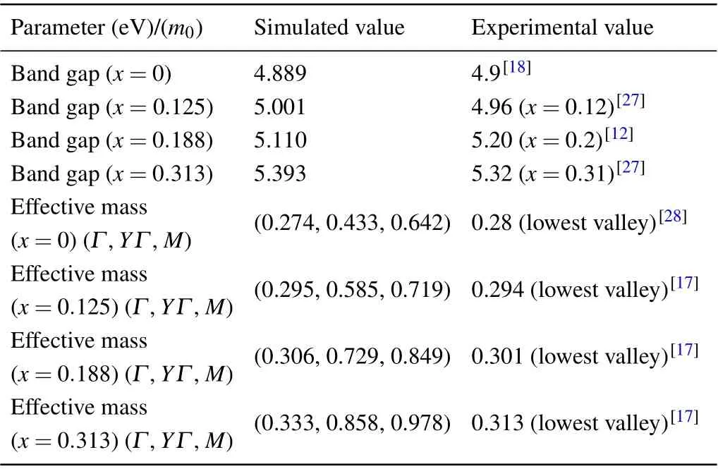
Table 1. Material parameters for β-(AlxGa1-x)2O3.
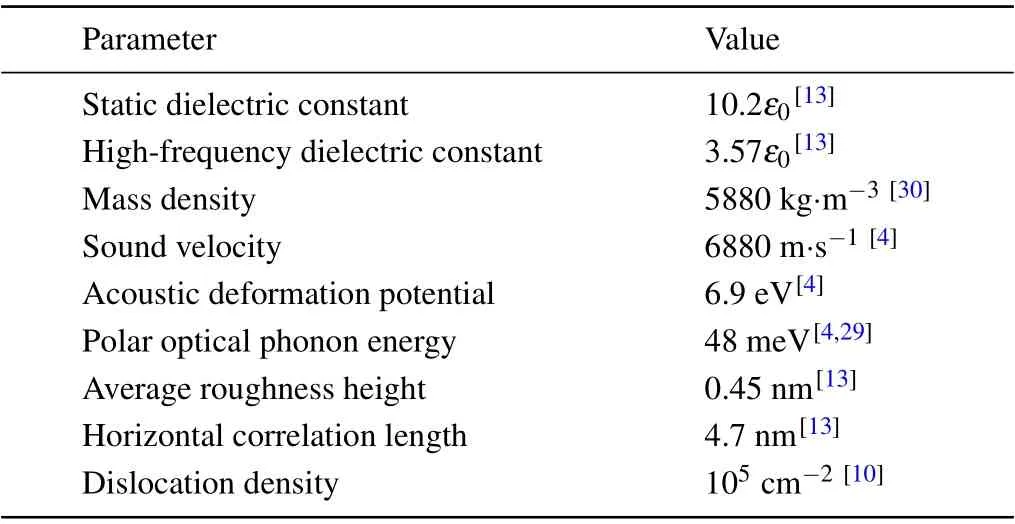
Table 2. Main material parameters.
In our MC simulation,the critical features of the conduction bands are theΓ,YΓ,andMvalleys. The quantization effect is considered only in theΓvalley with the five lowest subbands. The material parameters[4,10,13,29,30]used in the calculations are listed in Table 2. To compute the scattering rates of the 2DEG,the energy levels and wave functions are achieved by self-consistently solving the Schr¨odinger–Poisson equations. The scattering mechanisms include interface roughness scattering (IRS), polar optical phonon scattering (POP), alloy disorder scattering(ADS),acoustic deformation potential scattering (ADP) and dislocation scattering (DIS). Then the total mobility can be obtained using Matthiesen’s rule. The main processes of the calculation are described below.
Within the framework of the effective mass approximation,the Schr¨odinger equation can be written as

whereeis the electronic charge,φ(z)is the electrostatic potential and ΔEc(z)is the conduction band discontinuity at theβ-(AlxGa1-x)2O3/Ga2O3interface.[31]Then, the Poisson equation is written as

whereε(z)is the dielectric constant. The electron concentrationn(z)in the quantum well can be obtained as
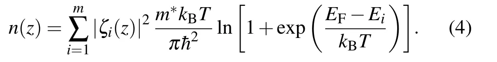
Here,mis the number of occupied subbands,kBis the Boltzmann constant,Tis the temperature andEFis the Fermi level.
When manufacturing heterostructures the roughness of the interface between different materials cannot be completely avoided,thus the IRS must be considered. The inverse of the momentum relaxation timeτlimited by IRS can be expressed by
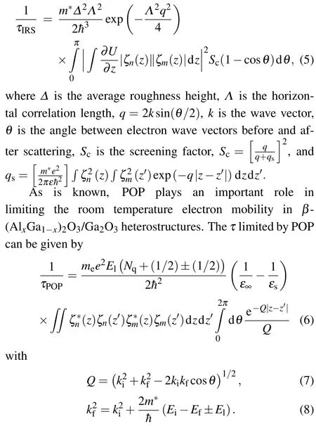
Here,meis the effective mass ofβ-Ga2O3andElis the polar optical photon energy, the value of which is based on the fitting of experimental data. Inβ-Ga2O3, although there are eight longitudinal optical phonon modes in a(100)direction,it can be found that a POP energy of 48 meV is good enough to capture the POP effect based on the Fr¨ohlich model.[4,13]Nqis the phonon occupation number,ε∞is the high-frequency dielectric constant,εsis the static dielectric constant,kiandkfare the wave vectors of the initial and final states,respectively,‘+’ represents phonon absorption and ‘–’ represents phonon emission.
3. Analysis and discussion
To investigate the electron transport properties ofβ-(AlxGa1-x)2O3/Ga2O3, the mobility of this heterostructure is studied first and the microscopic behaviors such as electron velocity and electron occupancy then discussed to further understand the transport phenomena ofβ-(AlxGa1-x)2O3/Ga2O3and the corresponding mechanisms.Finally,on the basis of the obtained velocity and displacement of the electrons,the diffusion coefficient is studied. In this work, all the properties are discussed at different temperatures or electric field strengths.
As is known, mobility is an important parameter for semiconductor devices such as transistors because it determines the power dissipation and switching speed.[32]To simulate the mobility properties ofβ-(AlxGa1-x)2O3/Ga2O3,some key parameters of the conduction band are required.The calculated conduction band profile, the first subband energy level and the corresponding wave function forβ-(Al0.188Ga0.812)2O3/Ga2O3are demonstrated in Fig. 2(a).Confinement of the 2DEG at the interface leads to the formation of energy subbands because of the quantization of the electronic band structure.[21]The ground wave function is well localized with some penetration to the potential barrier due to the finite conduction band offsets, which may induce ADS.The variation of the calculated electron mobility in aβ-(Al0.188Ga0.812)2O3/Ga2O3heterostructure with temperature is displayed in Fig.2(b). The reported theoretical and experimental results[13,15,16,19]are also provided for comparison. As can be observed,when IRS,POP and ADP are separately considered, the corresponding electron mobility calculated is in accordance with the reported theoretical result. When all five different scattering mechanisms are included, the calculated 2DEG electron mobility (the solid green line in Fig. 2(b))matches well with the experimental data at 100 K–300 K.However,at low temperatures the calculated mobility is higher than that in the experiment,mainly because the remote impurity scattering (RI) and background impurity scattering (BI)have a great impact on the doped heterostructures in the experiment. This effect is negligible for the unintentionally doped heterostructure in our model; therefore, when the contributions of RI and BI are removed, the calculated electron mobility is in good agreement with the experimental data,thus confirming the validity of our model. Figures 2(c) and 2(d)illustrate the electron mobility ofβ-(AlxGa1-x)2O3/Ga2O3with different Al compositions versus the applied electric field by MC simulation at different temperatures. In Fig. 2(c), the mobility decreases with the increase in the temperature for a fixed electric field,and the mobility for 10 kV·cm-1at 300 K is approximately 153.669 cm2·V-1·s-1. This is because the total scattering rate increases with increasing temperature.The electron mobility at room temperature decreases with the increasing Al composition when the electric field remains constant in Fig. 2(d), which is due to the fact that the impacts of ADS, DIS, and IRS are strengthened by the increasing Al content.[33]

Fig.2. (a)Calculated energy band profile,ground state subband energy level and the corresponding wave function of a β-(Al0.188Ga0.812)2O3/Ga2O3 quantum well at 300 K.(b)β-(Al0.188Ga0.812)2O3/Ga2O3 low-field electron mobility as a function of temperature. The solid lines and dashed lines with symbols represent the theoretical data,and the scatter dots denote the experimental data. Electron mobility as a function of the applied electric field in(c)β-(Al0.188Ga0.812)2O3/Ga2O3 at different temperatures and(d)β-(AlxGa1-x)2O3/Ga2O3 with different Al compositions at 300 K.

Fig. 3. Electron steady-state drift velocity as a function of the applied electric field in (a) β-(Al0.188Ga0.812)2O3/Ga2O3at different temperatures,and(b)β-(AlxGa1-x)2O3/Ga2O3with varying Al compositions at 300 K.The dashed lines with symbols represent the steady-state drift velocity of β-Ga2O3. (c)–(f)Electrons’occupancy as a function of the applied electric field in β-(Al0.188Ga0.812)2O3/Ga2O3at different temperatures.
To gain a good understanding of the electron mobility characteristic ofβ-(AlxGa1-x)2O3/Ga2O3heterostructures,the microscopic behavior of the electrons must be investigated in depth. As is known, steady-state electron transport is the dominant transport mechanism in devices with larger dimensions. For devices with smaller dimensions, however, transient electron transport must also be considered when evaluating device performance. Therefore, both the electron steadystate drift velocity and the electron transient velocity ofβ-(AlxGa1-x)2O3/Ga2O3were investigated in this work.
The electron drift velocity versus electric field ofβ-(AlxGa1-x)2O3/Ga2O3heterostructures is shown in Figs.3(a)and 3(b). In Fig.3(a),both the peak and the saturation velocities are dependent on temperature. This is because the POP rate increases significantly with increasing temperature. Besides, at a fixed temperature, the dependence of the drift velocity on electric field is almost linear at low electric fields.After the electron drift velocity reaches its peak value, the velocity decreases in response to further increase in the applied electric field. This behavior is a clear evidence of negative differential mobility (NDM). NDM occurs because electrons in theΓvalley will accelerate under high fields and gain enough energy to transfer to the satellite valleys. As can be seen in the electron occupancy curves in Figs. 3(c)–3(f),the inter-valley deformation scattering becomes effective when the electrons significantly populate the satellite valleys,and the effective masses of the satellite valleys are higher than that of theΓvalley. Then, with a continued increase in electric field, the short-range intra-valley electron–phonon interaction would result in saturation of the velocity.[34]Specifically, at 300 K with an electric field of 150 kV·cm-1, the maximum drift velocity is 1.197×107cm·s-1. This implies thatβ-(AlxGa1-x)2O3/Ga2O3can tolerate a high voltage with steady performance. Figure 3(b) gives the electron drift velocity versus electric field ofβ-Ga2O3for comparison. As can be observed, when the electric field is within 100 kV·cm-1, the steady-state drift velocities of bothβ-Ga2O3andβ-(AlxGa1-x)2O3/Ga2O3increase almost linearly with increasing electric field. The average drift velocity decreases with the increasing Al content. This situation is due to the increase in 2DEG density induced by the increasing Al content:an increasing number of electrons are electrostatically pushed closer to the heterointerface and the impact of IRS will be enhanced.
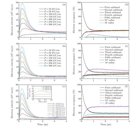
Fig.4. Transient electron velocity as a function of the applied electric field in β-(Al0.188Ga0.812)2O3/Ga2O3 at(a)77 K,(b)150 K,and(c)300 K.Inset: the transient electron velocity of β-Ga2O3 (results from Ref.[5]). The electron occupancy of β-(Al0.188Ga0.812)2O3/Ga2O3 as a function of time at 300 K with an applied electric field of(d)50 kV·cm-1,(e)150 kV·cm-1,and(f)300 kV·cm-1.
The electron transient characteristics ofβ-(Al0188Ga0.812)2O3/Ga2O3heterostructure are presented in Fig.4. Figures 4(a)–4(c)show the transient electron velocity versus the applied electric field at different temperatures. In the inset of Fig.4(c)the electron transient velocity versus time forβ-Ga2O3is given for comparison. As can be seen,the critical electric fields corresponding to the significant overshoot ofβ-(AlxGa1-x)2O3/Ga2O3andβ-Ga2O3are 100 kV·cm-1and 300 kV·cm-1,respectively. Besides,for the same electric field the peak transient velocities ofβ-Ga2O3are lower than those ofβ-(AlxGa1-x)2O3/Ga2O3. The overshoot is mainly because the momentum relaxation time is much lower than the energy relaxation time,and the time required for the transient process is of the same order of magnitude as the energy relaxation time. It can also be observed that the peak transient velocities are much higher than the peak velocities of electron steady-state drift properties in Fig. 3(a) under the same conditions. This is because in the ballistic regime the electrons can acquire energy from the applied field without losing energy to the lattice from scattering, and their velocity will reach a higher value than in the steady state.[35]Figures 4(d)–4(f) show the time evolution of the electron occupancy inβ-(Al0.188Ga0.812)2O3/Ga2O3at 300 K for different electric fields. It can be seen that the population of electrons in the first subband decreases at the beginning and that in higher subbands gradually increases. However, most electrons are still in theΓvalley, therefore the drift velocity initially increases,as shown in Fig. 4(c). As time progresses, electron excitation to the higher subbands and valleys begins to dominate,causing a decrease in the drift velocity. This phenomenon has also been observed in MgZnO/ZnO heterostructures by MC simulation.[33]
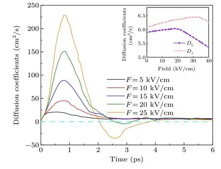
Fig. 5. Longitudinal diffusion coefficients as a function of time for β-(Al0.188Ga0.812)2O3/Ga2O3 at 300 K for different applied electric fields. Inset: longitudinal and transverse diffusion coefficients as a function of the applied electric field for β-(Al0.188Ga0.812)2O3/Ga2O3 at 300 K.
It is known that diffusion arises from the correlation between the velocity and displacement of particles, and the diffusion coefficient is of great significance in the study of the effect of carrier diffusion on the microwave characteristics of integratedβ-(AlxGa1-x)2O3/Ga2O3devices.[36]Figure 5 presents the longitudinal diffusion coefficient (D‖) versus time for different electric fields at room temperature. As can be seen,D‖sharply increases within the first 1 ps, then decreases with time and finally approaches zero. Because the diffusion coefficient is related to the correlation function of the velocity fluctuation for electrons,[36]and the transient electron velocityVtwill lose its correlation withVt=0 with time due to the irregular fluctuations of the velocity inβ-(Al0.188Ga0.812)2O3/Ga2O3. The inset showsD‖and the transverse diffusion coefficient (D⊥) versus electric field forβ-(Al0.188Ga0.812)2O3/Ga2O3at 300 K.D‖ <D⊥in the whole range of electric field is caused by the anisotropic effect of the crystallographic orientation.[37]This phenomenon is a significant feature of multivalley semiconductors[36]and can also be found in GaAs by MC investigation.[38]
4. Conclusion
In summary, a three-valley ensemble MC simulation is presented for detailed investigation of the electron transport characteristics ofβ-(AlxGa1-x)2O3/Ga2O3heterostructures.The electronic band structures are obtained by first-principles calculations, and the results are important parameters used in our simulations. Considering the quantization effects in theΓvalley, the wave functions and energy levels are obtained by iterative calculation and then used to compute the scattering rates of the 2DEG. The achieved electron mobility matches well with the experimental data, therefore proving the validity of our models. Forβ-(AlxGa1-x)2O3/Ga2O3, the electron mobility decreases when the Al content increases for a fixed electric field. A region of negative differential mobility can be observed in the velocity–field characteristics.At room temperature, the steady-state electron velocity could reach the order of 107cm·s-1at 150 kV·cm-1. Furthermore, a pronounced anisotropy of the diffusion coefficient is found. This work provides detailed information regarding the transport properties ofβ-(AlxGa1-x)2O3/Ga2O3,which is essential knowledge that will benefit the design and fabrication of high-qualityβ-(AlxGa1-x)2O3/Ga2O3heterostructure-based devices.
Acknowledgments
Project supported by the National Natural Science Foundation of China(Grant No.61474090),the Key Research and Development Program of Shaanxi Province of China (Grant No. 2017ZDXM-GY-052), and the Fundamental Research Funds for the Central Universities(Grant No.20109205456),and the Innovation Fund of Xidian University.
猜你喜欢
上海故事(2022年8期)2022-11-09
作物学报(2022年1期)2022-11-05
党员干部之友(2022年10期)2022-10-10
方圆(2022年12期)2022-09-15
方圆(2022年13期)2022-09-14
金山(2020年5期)2020-05-20
廉政瞭望(2019年5期)2019-06-10
故事林(2017年17期)2017-09-12
小说月刊(2017年7期)2017-07-10
意林·作文素材(2016年10期)2016-06-17

- Chinese Physics B的其它文章
- A design of resonant cavity with an improved coupling-adjusting mechanism for the W-band EPR spectrometer
- Photoreflectance system based on vacuum ultraviolet laser at 177.3 nm
- Topological photonic states in gyromagnetic photonic crystals:Physics,properties,and applications
- Structure of continuous matrix product operator for transverse field Ising model: An analytic and numerical study
- Riemann–Hilbert approach and N double-pole solutions for a nonlinear Schr¨odinger-type equation
- Diffusion dynamics in branched spherical structure